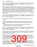
When the area 5 space is accessed and ordinary memory is connected, the CS5 signal is asserted.
The RD signal that can be used as OE and the WE0–WE3 signals for write control are also
asserted. When the PCMCIA interface is used, the CE1A signal, CE2A signal, RD signal as OE
signal, and WE1 signal are asserted.
The number of bus cycles is selected between 0 and 10 wait cycles using the A5W2–A5W0 bits in
WCR2. With the PCMCIA interface, from 0 to 38 wait cycles can be selected using the A5W2–
A5W0 bits in WCR2 and the A5W3 bit in PCR. In addition, any number of waits can be inserted
in each bus cycle by means of the external wait pin (WAIT). When a burst function is used, the
bus cycle pitch of the burst cycle is determined within a range of 2–11 (2–39 for the PCMCIA
interface) according to the number of waits. The setup and hold times of address/CS5 for the
read/write strobe signals can be set in the range 0.5–7.5 using bits A5TED2–A5TED0 and
A5TEH2–A5TEH0 in the PCR register.
Area 6: Area 6 physical address bits A28–A26 are 110. Address bits A31–A29 are ignored and
the address range is the 64 Mbytes at H'18000000 + H'20000000 × n – H'1BFFFFFF +
H'20000000 × n (n = 0–6 and n = 1–6 are the shadow spaces).
Ordinary memories such as SRAM and ROM as well as burst ROM and PCMCIA interfaces can
be connected to this space. When the PCMCIA interface is used, the IC memory card interface
address range is 32 Mbytes at H'18000000 + H'20000000 × n – H'19FFFFFF + H'20000000 × n
and the I/O card interface address range is 32 Mbytes at H'1A000000 + H'20000000 × n –
H'1BFFFFFF + H'20000000 × n (n = 0–6 and n = 1–6 are the shadow spaces).
For ordinary memory and burst ROM, byte, word, or longword can be selected as the bus width
using bits A6SZ1 and A6SZ0 in BCR2. For the PCMCIA interface, byte or word can be selected
as the bus width using bits A6SZ1 and A6SZ0 in BCR2.
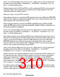
When the area 6 space is accessed and ordinary memory is connected, the CS6 signal is asserted.
The RD signal that can be used as OE and the WE0–WE3 signals for write control are also
asserted. When the PCMCIA interface is used, the CE1B signal, CE2B signal, RD signal as OE
signal, and WE, ICIORD, and ICIOWR signals are asserted.
The number of bus cycles is selected between 0 and 10 wait cycles using the A6W2–A6W0 bits in
WCR2. With the PCMCIA interface, from 0 to 38 wait cycles can be selected using the A6W2–
A6W0 bits in WCR2 and the A6W3 bit in PCR. In addition, any number of waits can be inserted
in each bus cycle by means of the external wait pin (WAIT). The bus cycle pitch of the burst cycle
is determined within a range of 2–11 (2–39 for the PCMCIA interface) according to the number of
waits. The address/CS6 setup and hold times for the read/write strobe signals can be set in the
range 0.5–7.5 using bits A6TED2–A6TED0 and A6TEH2–A6TEH0 in the PCR register.
Rev. 5.00, 09/03, page 267 of 760

 RENESAS [ RENESAS TECHNOLOGY CORP ]