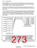
10.1.5 Area Overview
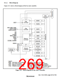
Space Allocation: In the architecture of the SH7709S, both logical spaces and physical spaces
have 32-bit address spaces. The logical space is divided into five areas by the value of the upper
bits of the address. The physical space is divided into eight areas.
Logical space can be allocated to physical space using a memory management unit (MMU). For
details, refer to section 3, Memory Management Unit (MMU), which describes area allocation for
physical space.
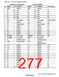
As shown in table 10.3, the SH7709S can be connected directly to six memory/PCMCIA interface
areas, and it outputs chip select signals (CS0, CS2–CS6, CE2A, CE2B) for each of them. CS0 is
asserted during area 0 access; CS6 is asserted during area 6 access. When PCMCIA interface is
selected in area 5 or 6, in addition to CS5/CS6, CE2A/CE2B are asserted for the corresponding
bytes accessed.
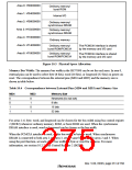
H'00000000
Area 0 (CS0)
Internal I/O
H'00000000
H'04000000
H'08000000
H'0C000000
H'10000000
H'14000000
H'18000000
H'20000000
H'40000000
H'60000000
H'80000000
Area 2 (CS2)
Area 3 (CS3)
Area 4 (CS4)
Area 5 (CS5)
Area 6 (CS6)
Reserved area
P0, U0
P1
P2
P3
P4
Physical address space
H'A0000000
H'C0000000
H'E0000000
Logical address space
Note: For logical address spaces P0 and P3, when the memory management unit (MMU) is
on, it can optionally generate a physical address for the logical address. This diagram
can be applied when the MMU is off, and when the MMU is on and each physical
address corresponding to a logical address is equal except for the upper three bits.
When translating logical addresses to arbitrary physical addresses, refer to table 10.3.
Figure 10.2 Correspondence between Logical Address Space and Physical Address Space
Rev. 5.00, 09/03, page 229 of 760

 RENESAS [ RENESAS TECHNOLOGY CORP ]