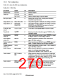
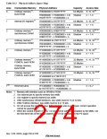
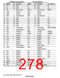
Table 10.3 Physical Address Space Map
Area
Connectable Memory
Physical Address
Capacity
Access Size
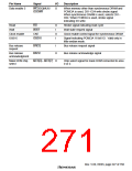
1
2
*
*
0
Ordinary memory ,
H'00000000 to H'03FFFFFF
64 Mbytes 8, 16, 32
burst ROM
H'00000000 + H'20000000 × n to Shadow
H'03FFFFFF + H'20000000 × n
n = 1–6
7
3
*
*
1
2
3
4
5
Internal I/O registers
H'04000000 to H'07FFFFFF
64 Mbytes 8, 16, 32
H'04000000 + H'20000000 × n to Shadow
H'07FFFFFF + H'20000000 × n
n = 1–6
*3 *4
1
*
Ordinary memory ,
H'08000000 to H'0BFFFFFF
64 Mbytes 8, 16, 32
synchronous DRAM
H'08000000 + H'20000000 × n to Shadow
H'0BFFFFFF + H'20000000 × n
n = 1–6
*3 *4
1
*
Ordinary memory ,
H'0C000000 to H'0FFFFFFF
64 Mbytes 8, 16, 32
synchronous DRAM
H'0C000000 + H'20000000 × n to Shadow
H'0FFFFFFF + H'20000000 × n
n = 1–6
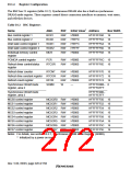
1
3
*
*
Ordinary memory
H'10000000 to H'13FFFFFF
64 Mbytes 8, 16, 32
H'10000000 + H'20000000 × n to Shadow
H'13FFFFFF + H'20000000 × n
n = 1–6
1
*
*3 *5
Ordinary memory ,
H'14000000 to H'15FFFFFF
H'16000000 to H'17FFFFFF
32 Mbytes 8, 16, 32
32 Mbytes
PCMCIA, burst ROM
Ordinary memory,
burst ROM
H'14000000 + H'20000000 × n to Shadow
H'17FFFFFF + H'20000000 × n
n = 1–6
1
*
*3 *5
6
Ordinary memory ,
H'18000000 to H'19FFFFFF
H'1A000000 to H'1BFFFFFF
32 Mbytes 8, 16, 32
PCMCIA, burst ROM
H'18000000 + H'20000000 × n to Shadow
H'1BFFFFFF + H'20000000 × n
n = 1–6
n = 0–7
6
*
7
Reserved area
H'1C000000 + H'20000000 × n
to H'1FFFFFFF + H'20000000 × n
Notes: 1. Memory with interface such as SRAM or ROM.
2. Use external pin to specify memory bus width.
3. Use register to specify memory bus width.
4. With synchronous DRAM interfaces, bus width must be 16 or 32 bits.
5. With PCMCIA interface, bus width must be 8 or 16 bits.
6. Do not access the reserved area. If the reserved area is accessed, correct operation
cannot be guaranteed.
7. When the control register in area 1 is not used for address translation by the MMU, set
the first three bits of the logical address to 101 for allocation to the P2 space.
Rev. 5.00, 09/03, page 230 of 760

 RENESAS [ RENESAS TECHNOLOGY CORP ]