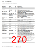
Pin Name
Signal
I/O
Description
Data enable 3
WE3/DQMUU/
O
When memory other than synchronous DRAM and
PCMCIA is used, D31–D24 write strobe signal.
When synchronous DRAM is used, selects D31–
D24. When PCMCIA is used, strobe signal
indicating I/O write.
ICIOWR
Read
RD
WAIT
CKE
O
I
Strobe signal indicating read cycle
Wait state request signal
Wait
Clock enable
IOIS16
O
I
Clock enable control signal for synchronous DRAM
IOIS16
Signal indicating PCMCIA 16-bit I/O. Valid only in
little-endian mode.
Bus release
request
BREQ
BACK
I
Bus release request signal
Bus release
acknowledgment
O
Bus release acknowledge signal
Mask ROM chip
select
MCS[0]– MCS[7] O
Chip select signal for mask ROM connected to area
0 or 2.
Rev. 5.00, 09/03, page 227 of 760

 RENESAS [ RENESAS TECHNOLOGY CORP ]