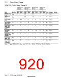
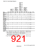
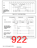
22.3.2 Control Signal Timing
Table 22.34 Control Signal Timing (1)
HD6417750
RBP240
HD6417750
RBP200
HD6417750
RF240
HD6417750
RF200
*
*
*
*
Item
Symbol Min Max
Min Max
Min Max
Min Max Unit Figure Notes
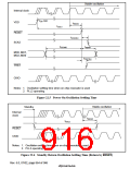
%5(4 setup tBREQS
2
—
—
5.3
12
2
2.5
1.5
—
—
—
6
3.5
1.5
—
—
—
6
3.5
1.5
—
—
—
6
ns
ns
ns
ns
tcyc
22.13
22.13
22.13
22.13
22.14
time
%5(4 hold
tBREQH
1.5
—
—
—
time
%$&. delay tBACKD
time
Bus tri-state
delay time
tBOFF1
tBOFF2
—
12
2
—
12
2
—
12
2
Bus tri-state
delay time
to standby
mode
—
—
—
Bus buffer
on time
tBON1
tBON2
—
—
12
1
—
—
12
1
—
—
12
1
—
—
12
1
ns
tcyc
22.13
22.14
Bus buffer
on time from
standby
STATUS0/1
delay time
tSTD1
tSTD2
—
—
5
2
—
—
6
2
—
—
6
2
—
—
6
2
ns
tcyc
22.14
22.14
STATUS0/1
delay time
to standby
Note: * VDDQ = 3.0 to 3.6 V, VDD = typ. 1.5 V, Ta = –20 to +75°C, CL = 30 pF, PLL2 on
Rev. 6.0, 07/02, page 868 of 986

 RENESAS [ RENESAS TECHNOLOGY CORP ]