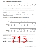
Bit 4—Receive Enable (RE): Enables or disables the start of serial reception by the SCIF.
Bit 4: RE
Description
1
*
0
1
Reception disabled
(Initial value)
2
*
Reception enabled
Notes: *1 Clearing the RE bit to 0 does not affect the DR, ER, BRK, RDF, FER, PER, and ORER
flags, which retain their states.
*2 Serial transmission is started when a start bit is detected in this state.
Serial mode register (SCSMR2) and FIFO control register (SCFCR2) settings must be
made, the reception format decided, and the receive FIFO reset, before the RE bit is set
to 1.
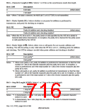
Bit 3—Receive Error Interrupt Enable (REIE): Enables or disables generation of receive-error
interrupt (ERI) and break interrupt (BRI) requests. The REIE bit setting is valid only when the
RIE bit is 0.
Bit 3: REIE
Description
0
Receive-error interrupt (ERI) and break interrupt (BRI) requests disabled*
(Initial value)
1
Receive-error interrupt (ERI) and break interrupt (BRI) requests enabled
Note: * Receive-error interrupt (ERI) and break interrupt (BRI) requests can be cleared by reading 1
from the ER, BRK, or ORER flag, then clearing the flag to 0, or by clearing the RIE and
REIE bits to 0. When REIE is set to 1, ERI and BRI interrupt requests will be generated
even if RIE is cleared to 0. In DMAC transfer, this setting is made if the interrupt controller is
to be notified of ERI and BRI interrupt requests.
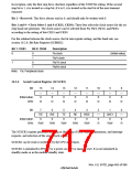
Bit 1—Clock Enable 1 (CKE1): Selects the SCIF clock source. The CKE1 bit must be set before
determining the SCIF’s operating mode with SCSMR2.
Bit 1: CKE1
Description
0
1
Internal clock/SCK2 pin functions as port
External clock/SCK2 pin functions as clock input*
(Initial value)
Note: * Inputs a clock with a frequency 16 times the bit rate.
Rev. 6.0, 07/02, page 667 of 986

 RENESAS [ RENESAS TECHNOLOGY CORP ]