13.3.12 Master Mode
The master mode processor holds the bus itself unless it receives a bus request.
On receiving an assertion (low level) of the bus request signal (%5(4) from off-chip, the master
mode processor releases the bus and asserts (drives low) the bus use permission signal (%$&.) as
soon as the currently executing bus cycle ends. If a bus release request due to a refresh request has
not been issued, on receiving the %5(4 negation (high level) indicating that the slave has released
the bus, the processor negates (drives high) the %$&. signal and resumes use of the bus.
If a bus request is issued due to a memory refresh request in the bus-released state, the processor
negates the bus use permission signal (%$&.), and on receiving the %5(4 negation indicating
that the slave has released the bus, resumes use of the bus.
When the bus is released, all bus interface related output signals and input/output signals go to the
high-impedance state, except for the synchronous DRAM interface CKE signal and bus arbitration
%$&. signal, and DACK0 and DACK1 which control DMA transfers.
With DRAM, the bus is released after precharging is completed. With synchronous DRAM, also,
a precharge command is issued for the active bank and the bus is released after precharging is
completed.
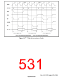
The actual bus release sequence is as follows.
First, the bus use permission signal is asserted in synchronization with the rising edge of the clock.
The address bus and data bus go to the high-impedance state in synchronization with the next
rising edge of the clock after this %$&. assertion. At the same time, the bus control signals (%6,
&6Q, 5$64, 5$65, :(Q, 5', RD/:5, 5'5, RD/:55, &(5$, and &(5%) go to the high-
impedance state. These bus control signals are negated no later than one cycle before going to
high-impedance. Bus request signal sampling is performed on the rising edge of the clock.
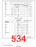
The sequence for re-acquiring the bus from the slave is as follows.
As soon as %5(4 negation is detected on the rising edge of the clock, %$&. is negated and bus
control signal driving is started. Driving of the address bus and data bus starts at the next rising
edge of an in-phase clock. The bus control signals are asserted and the bus cycle is actually
started, at the earliest, at the clock rising edge at which the address and data signals are driven.
In order to reacquire the bus and start execution of a refresh operation or bus access, the %5(4
signal must be negated for at least two cycles.
If a refresh request is generated when %$&. has been asserted and the bus has been released, the
%$&. signal is negated even while the %5(4 signal is asserted to request the slave to relinquish
the bus. When the SH7750 Series is used in master mode, consecutive bus accesses may be
attempted to reduce the overhead due to arbitration in the case of a slave designed independently
Rev. 6.0, 07/02, page 483 of 986

 RENESAS [ RENESAS TECHNOLOGY CORP ]