13.3.14 Partial-Sharing Master Mode
In partial-sharing master mode, area 2 only is shared with other devices, and other areas can be
accessed at all times. Partial-sharing master mode can be set by setting master mode with the
external mode pins, and setting the PSHR bit to 1 in BCR1 in the initialization procedure in a
power-on reset. In a manual reset the bus state controller setting register values are retained, and
so need not be set again.
Partial-sharing master mode is designed for use in conjunction with a master mode chip. The
partial-sharing master can access a device on the master side via area 2, but the master cannot
access a device on the partial-sharing master side.
An address and control signal buffer and a data buffer must be located between the partial-sharing
master and the master, and controlled by a buffer control circuit.
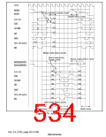
The partial-sharing master mode processor uses the following procedure to access area 2. It asserts
the %65(4 signal on the rising edge of the clock, and issues a bus request to the master. It
samples %6$&. on each rising edge of the clock, and on receiving %6$&. assertion, starts the
access cycle on the next rising edge of the clock. At the end of the access, it negates %65(4 on
the rising edge of the clock. Buffer control in an access to an area 2 device by the partial-sharing
master is carried out by referencing the &65 signal or %65(4 and %6$&. signals on the partial-
sharing master side. Permission to use the bus is reported by the %6$&. line connected to the
partial-sharing master, but the master may also negate the %6$&. signal even while the bus is
being used, if it needs the bus urgently in order to service a refresh, for example. Consequently,
the partial-sharing master has to monitor the %65(4 signal to see whether it can continue to use
the bus after detecting %6$&. assertion. In the case of the address buffer, after the address buffer
is turned on when %6$&. assertion is detected, the buffer is kept on until %65(4 is negated, at
which point it is turned off. If the turning-off of the buffer used is late, resulting in a collision with
the start of an access cycle on the master side, the %65(4 signal output from the partial-sharing
master must be routed through a delay circuit as part of the buffer control circuit, and input to the
master %5(4 signal.
In order for a partial-sharing master mode processor to begin area 2 access, the %6$&. signal
must be asserted for at least two cycles.
When the bus is released after area 2 has been accessed in partial-sharing master mode, if area 2 is
synchronous DRAM, there is a wait of the period required for auto-precharge before bus release is
performed.
In partial-sharing master mode, refreshing is not performed for area 2 (refresh requests are
ignored).
Do not use DRAM/synchronous DRAM RAS down mode in partial-sharing master mode.
Rev. 6.0, 07/02, page 485 of 986

 RENESAS [ RENESAS TECHNOLOGY CORP ]