control register (PCR), are selected. When the TC bit to be accessed is set to 1, bits A6W2 to
A6W0 in wait control register 2 (WCR2), and bits A6PCW1 and A6PCW0, A6TED2 to A6TED0,
and A6TEH2 to A6TEH0 in the PCMCIA control register (PCR), are selected. For the method of
setting bits SA2 to SA0 and bit TC for the page to be accessed, see section 3, Memory
Management Unit (MMU).
In the SH7750S and SH7750R, the PCMCIA interface can be accessed even when the MMU is
not used. When the MMU is off (MMUCR.AT=0), access is always performed by means of bits
SA2 to SA0 and bit TC in the page table entry assistance register (PTEA). When the MMU is on
(MMUCR.AT=1), the situation is the same as for the SH7750.
In the SH7750 Series, access to a PCMCIA interface area by the DMAC is always performed
using the DMAC’s CHCRn.SSAn, CHCRn.DSAn, CHCRn.STC, and CHCRn.DTC values.
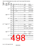
SA2
SA1
SA0
0
Description
0
0
Reserved (Setting prohibited)
Dynamic I/O bus sizing
8-bit I/O space
1
1
0
1
0
1
16-bit I/O space
1
0
8-bit common memory
16-bit common memory
8-bit attribute memory
16-bit attribute memory
1
0
1
AnPCW1–AnPCW0 specify the number of wait states to be inserted in a low-speed bus cycle; a
value of 0, 15, 30, or 50 can be set, and this value is added to the number of wait states for
insertion specified by WCR2. AnTED2–AnTED0 can be set to a value from 0 to 15, enabling the
address, &6, &(5$, &(5%, and 5(* setup times with respect to the 5' and :(4 signals to be
secured. AnTEH2–AnTEH0 can also be set to a value from 0 to 15, enabling the address, &6,
&(5$, &(5%, and 5(* write data hold times with respect to the 5' and :(4 signals to be
secured.
Wait cycles between cycles are set with bits A5IW2–A5IW0 and A6IW2–A6IW0 in wait control
register 1 (WCR1). The inter-cycle write cycles selected depend only on the area accessed (area 5
or 6): when area 5 is accessed, bits A5IW2–A5IW0 are selected, and when area 6 is accessed, bits
A6IW2–A6IW0 are selected.
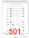
In 32-byte transfer, a total of 32 bytes are transferred consecutively according to the set bus width.
The first access is performed on the data for which there was an access request, and the remaining
accesses are performed on the data at the 32-byte boundary. The bus is not released during this
period.
Rev. 6.0, 07/02, page 445 of 986

 RENESAS [ RENESAS TECHNOLOGY CORP ]