•
•
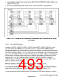
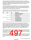
Control signals required in this connection are 5$6, &$6, RD/:5, &66, DQM0−DQM7, and
CKE. &65 is not used.
Do not use partial-sharing mode. If you use this, correct operation is not guaranteed.
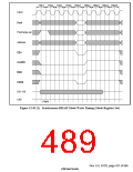
SH7750R
CKIO
CKE
CLK
CKE
CLK
CKE
CLK
CKE
CLK
CKE
CS3
RAS
CS
RAS
CS
RAS
CS
RAS
CS
RAS
CASS
RD/WR
A17
CAS
WE
CAS
WE
CAS
WE
CAS
WE
BANK1
BANK0
A12–A0
I/O15–I/O0
DQMU
DQML
BANK1
BANK0
A12–A0
I/O15–I/O0
DQMU
DQML
BANK1
BANK0
A12–A0
I/O15–I/O0
DQMU
DQML
BANK1
BANK0
A12–A0
I/O15–I/O0
DQMU
DQML
A16
A15–A3
D63–D48
DQM7
DQM6
D47–D32
DQM5
DQM4
D31–D16
DQM3
DQM2
D15–D0
DQM1
DQM0
Figure 13.45 Example of the Connection of Synchronous DRAM with 64-bit Bus Width
(256 Mbits)
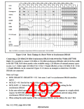
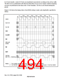
13.3.6 Burst ROM Interface
Setting bits A0BST2–A0BST0, A5BST2–A5BST0, and A6BST2–A6BST0 in BCR1 to a non-
zero value allows burst ROM to be connected to areas 0, 5, and 6. The burst ROM interface
provides high-speed access to ROM that has a burst access function. The timing for burst access to
burst ROM is shown in figure 13.46. Two wait cycles are set. Basically, access is performed in the
same way as for SRAM interface, but when the first cycle ends, only the address is changed before
the next access is executed. When 8-bit ROM is connected, the number of consecutive accesses
can be set as 4, 8, 16, or 32 with bits A0BST2–A0BST0, A5BST2–A5BST0, or A6BST2–
A6BST0. When 16-bit ROM is connected, 4, 8, or 16 can be set in the same way. When 32-bit
ROM is connected, 4 or 8 can be set.
5'< pin sampling is always performed when one or more wait states are set.
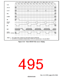
The second and subsequent access cycles also comprise two cycles when a burst ROM setting is
made and the wait specification is 0. The timing in this case is shown in figure 13.47.
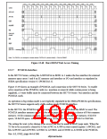
A write operation for the burst ROM interface is performed as if the SRAM interface is selected.
Rev. 6.0, 07/02, page 441 of 986

 RENESAS [ RENESAS TECHNOLOGY CORP ]