Power-On Sequence: In order to use synchronous DRAM, mode setting must first be performed
after powering on. To perform synchronous DRAM initialization correctly, the bus state controller
registers must first be set, followed by a write to the synchronous DRAM mode register. In
synchronous DRAM mode register setting, the address signal value at that time is latched by a
combination of the 5$6, &$6, and RD/:5 signals. If the value to be set is X, the bus state
controller provides for value X to be written to the synchronous DRAM mode register by
performing a write to address H'FF900000 + X for area 2 synchronous DRAM, and to address
H'FF940000 + X for area 3 synchronous DRAM. In this operation the data is ignored, but the
mode write is performed as a byte-size access. To set burst read/write, CAS latency 1 to 3, wrap
type = sequential, and burst length 4* or 8, supported by the SH7750, arbitrary data is written by
byte-size access to the following addresses.
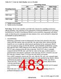
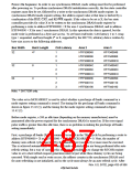
Bus Width
Burst Length
CAS Latency
Area 2
Area 3
32
4*
1
2
3
1
2
3
1
2
3
H'FF900048
H'FF900088
H'FF9000C8
H'FF90004C
H'FF90008C
H'FF9000CC
H'FF900090
H'FF900110
H'FF900190
H'FF940048
H'FF940088
H'FF9400C8
H'FF94004C
H'FF94008C
H'FF9400CC
H'FF940090
H'FF940110
H'FF940190
32
64
8
4
Note: * SH7750R only.
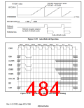
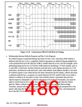
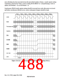
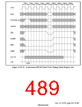
The value set in MCR.MRSET is used to select whether a precharge all banks command or a
mode register setting command is issued. The timing for the precharge all banks command is
shown in figure 13.42 (1), and the timing for the mode register setting command in figure
13.42 (2).
Before mode register, a 200 µs idle time (depending on the memory manufacturer) must be
guaranteed after the power required for the synchronous DRAM is turned on. If the reset signal
pulse width is greater than this idle time, there is no problem in making the precharge all banks
setting immediately.
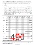
First, a precharge all banks (PALL) command is issued in the TRp1 cycle by performing a write to
address H'FF900000 + X or H'FF940000 + X while MCR.MRSET = 0. Next, the number of
dummy auto-refresh cycles specified by the manufacturer (usually 8) or more must be executed.
This is achieved automatically while various kinds of initialization are being performed after auto-
refresh setting, but a way of carrying this out more dependably is to change the RTCOR register
value to set a short refresh request generation interval just while these dummy cycles are being
executed. With simple read or write access, the address counter in the synchronous DRAM used
for auto-refreshing is not initialized, and so the cycle must always be an auto-refresh cycle. After
Rev. 6.0, 07/02, page 435 of 986

 RENESAS [ RENESAS TECHNOLOGY CORP ]