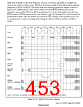
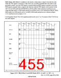
EDO Mode: With DRAM, in addition to the mode in which data is output to the data bus only
while the &$6 signal is asserted in a data read cycle, an EDO (extended data out) mode is also
provided in which, once the &$6 signal is asserted while the 5$6 signal is asserted, even if the
&$6 signal is negated, data is output to the data bus until the &$6 signal is next asserted. In the
SH7750, the EDO mode bit (EDOMODE) in MCR enables either normal access/burst access
using fast page mode, or EDO mode normal access/burst access, to be selected for DRAM. When
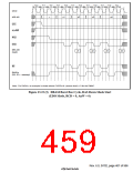
EDO mode is set, BE must be set to 1 in MCR. EDO mode normal access is shown in figure
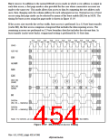
13.20, and burst access in figure 13.21.
CAS Negation Period: The CAS negation period can be set to 1 or 2 by means of the TCAS bit in
the MCR register.
Tr1
Tr2
Tc1
Tc2
Tce
Tpc
CKIO
Row
Column
A25–A0
RD/
D63–D0
(read)
DACKn
(SA: IO ← memory)
Note: For DACKn, an example is shown where CHCRn.AL (access level) = 0 for the DMAC.
Figure 13.20 DRAM Bus Cycle (EDO Mode, RCD = 0, AnW = 0, TPC = 1)
Rev. 6.0, 07/02, page 403 of 986

 RENESAS [ RENESAS TECHNOLOGY CORP ]