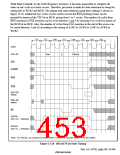
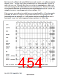
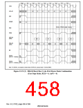
Burst Access: In addition to the normal DRAM access mode in which a row address is output in
each data access, a fast page mode is also provided for the case where consecutive accesses are
made to the same row. This mode allows fast access to data by outputting the row address only
once, then changing only the column address for each subsequent access. Normal access or burst
access using fast page mode can be selected by means of the burst enable (BE) bit in MCR. The
timing for burst access using fast page mode is shown in figure 13.19.
If the access size exceeds the set bus width, burst access is performed. In a 32-byte burst transfer
(cache fill), the first access comprises a longword that includes the data requiring access. The
remaining accesses are performed on 32-byte boundary data that includes the relevant data. In
burst transfer (cache write-back), wraparound writing is performed for 32-byte data.
Tr1
Tr2
Tc1
Tc2 Tc1 Tc2
Tc1
Tc2 Tc1 Tc2 Tpc
CKIO
r
c1
c2
c3
c4
A25–A0
RD/
D63–D0
(read)
d1
d2
d3
d4
D63–D0
(write)
d1
d4
d2
d3
DACKn
(SA: IO ← memory)
DACKn
(SA: IO → memory)
Note: For DACKn, an example is shown where CHCRn.AL (access level) = 0 for the DMAC.
Figure 13.19 DRAM Burst Access Timing
Rev. 6.0, 07/02, page 402 of 986

 RENESAS [ RENESAS TECHNOLOGY CORP ]