Bit 1 (SH7750S and SH7750R)—Module Stop 6 (MSTP6): Specifies that the clock supply to
the store queue (SQ) in the cache controller (CCN) is stopped. Setting the MSTP6 bit to 1 stops
the clock supply to the SQ, and the SQ functions are therefore unavailable.
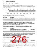
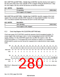
Bit 1: MSTP6
Description
0
1
SQ operating
(Initial value)
Clock supply to SQ stopped
Bit 0 (SH7750S and SH7750R)—Module Stop 5 (MSTP5): Specifies stopping of the clock
supply to the user break controller (UBC) among the on-chip peripheral modules. See section
20.6, User Break Controller Stop Functions for how to set the clock supply.
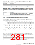
Bit 0: MSTP5
Description
0
1
UBC operating
(Initial value)
Clock supply to UBC stopped
9.2.5
Clock-Stop Register 00 (CLKSTP00) (SH7750R Only)
Clock-stop register 00 (CLKSTP00) controls the operation clock for peripheral modules. To
resume supply of the clock signal, write a 1 to the corresponding bit in the CLKSTPCLR00
register. Writing a 0 to the CLKSTP00 register does not affect the register’s value. The
CLKSTP00 register is a 32-bit register that can be read from or written to. It is initialized to
H'0000 0000 by a power-on reset, but not by a manual reset or when the device enters standby
mode.
Bit:
31
—
0
30
—
0
29
—
0
28
—
0
27
—
0
26
—
0
25
—
0
24
—
0
23
—
0
22
—
0
21
—
0
20
—
0
19
—
0
18
—
0
17
—
0
16
—
0
Initial value:
R/W:
R
R
R
R
R
R
R
R
R
R
R
R
R
R
R
R
Bit:
15
—
0
14
—
0
13
—
0
12
—
0
11
—
0
10
—
0
9
—
0
8
—
0
7
—
0
6
—
0
5
—
0
4
—
0
3
—
0
2
—
0
1
0
CSTP1 CSTP0
Initial value:
R/W:
0
0
R
R
R
R
R
R
R
R
R
R
R
R
R
R
R/W R/W
Bits 31 to 2—Reserved: Any data written to these bits should always be 0. These bits are always
read as 0.
Rev. 6.0, 07/02, page 228 of 986

 RENESAS [ RENESAS TECHNOLOGY CORP ]