9.1.2
Register Configuration
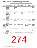
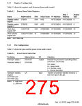
Table 9.2 shows the registers used for power-down mode control.
Table 9.2 Power-Down Mode Registers
Area 7
Initial Value P4 Address Address
Access
Size
Name
Abbreviation
R/W
Standby control STBCR
register
R/W
H'00
H'FFC00004 H'1FC00004
8
Standby control STBCR2
register 2
R/W
R/W
W
H'00
H'FFC00010 H'1FC00010
8
Clock stop
CLKSTP00
H'00000000 H'FE0A0000 H'1E0A0000 32
H'00000000 H'FE0A0008 H'1E0A0008 32
register 00*
Clock release
CLKSTPCLR00
register 00*
Note: * SH7750R only
9.1.3
Pin Configuration
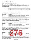
Table 9.3 shows the pins used for power-down mode control.
Table 9.3 Power-Down Mode Pins
Pin Name
Abbreviation
STATUS1
I/O
Function
Processor status 1
Processor status 0
Output
Indicate the processor’s operating status.
(STATUS1, STATUS0)
STATUS0
HH: Reset
HL: Sleep mode
LH: Standby mode
LL: Normal operation
Hardware standby
request
CA
Input
Transits to hardware standby mode by a
low-level input to the pin.
(SH7750S and
SH7750R only)
Notes: H: High level
L: Low level
Rev. 6.0, 07/02, page 223 of 986

 RENESAS [ RENESAS TECHNOLOGY CORP ]