CLOCK GENERATING CIRCUIT
4.2 Clocks
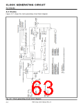
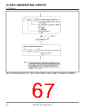
b7
b0
0
0
1 1 Clock control register 0 (Address BC16
)
PLL frequency multiplier is active, and pin
CONT is valid.
V
(Note 1)
PLL multiplication ratio select bits
b3 b2
0 1 : Double
1 0 : Triple
1 1 : Quadruple
System clock select bit
0 : fXIN
(Note 2)
N
2 ms elapsed ?
Y
Setting of system clock select bit to “1.”
b7
b0
Clock control register 0 (Address BC16
)
1
1
1
1
System clock select bit
0 : fPLL
Notes 1: After reset, these bits are allowed to be changed only once. If
it is necessary to write a certain value to these bits, be sure to
write the same value that has been written after the latest reset.
2: This decision is unnecessary If double is selected and the
period of RESET = “L” is “the oscillation stabilizing time of an
oscillator + 2 ms” or more.
Fig. 4.2.3 Setting procedure for clock control register 0 when using PLL frequency multiplier
7906 Group User’s Manual Rev.2.0
4-8

 RENESAS [ RENESAS TECHNOLOGY CORP ]