CLOCK GENERATING CIRCUIT
4.2 Clocks
4.2.2 Clock control register 0
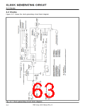
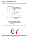
Figure 4.2.2 shows the structure of the clock control register 0, and Figure 4.2.3 shows the setting procedure
for the clock control register 0 when using the PLL frequency multiplier.
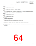
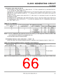
b7 b6 b5 b4 b3 b2 b1 b0
Clock control register 0 (Address BC16)
1
1
Bit
0
Bit name
Fix this bit to “1.”
Function
At reset
R/W
1
1
RW
RW
PLL circuit operation enable bit
1
0 : PLL frequency multiplier is inactive, and pin VCONT
is invalid. (Floating)
(Note 1)
1 : PLL frequency multiplier is active, and pin VCONT is valid.
b3 b2
RW
RW
1
0
2
3
PLL multiplication ratio select bits
0 0 : Do not select.
0 1 : ❈ 2
1 0 : ❈ 3
1 1 : ❈ 4
(Note 2)
RW
RW
4
5
1
0
Fix this bit to “1.”
System clock select bit
0 : fXIN
(Note 3) 1 : fPLL
See Table 4.2.2.
Peripheral device’s clock select bit 0
Peripheral device’s clock select bit 1
RW
RW
6
7
0
0
Notes 1: Clear this bit to “0” if the PLL frequency multiplier needs not to be active.
In the stop and flash memory parallel I/O modes, the PLL frequency multiplier is inactive and pin VCONT is invalid regard-
less of the contents of this bit.
2: Rewriting of these bits must be performed simultaneously with clearance of the system clock select bit (bit 5) to “0”. Then,
set bit 5 to “1” 2 ms after the rewriting of these bits. (After reset, these bits are allowed to be changed only once.)
3: Clearance of the PLL circuit operation enable bit (bit 1) to “0” clears the system clock select bit to “0.” Also, while the PLL
circuit operation enable bit = “0,” nothing can be written to the system clock select bit. (Fixed to be “0.”)
Before setting of set the system clock select bit to “1” after reset, it is necessary to insert an interval of 2 ms after the
stabilization of f(XIN).
Fig. 4.2.2 Structure of clock control register
(1) PLL circuit operation enable bit (bit 1)
Setting this bit to “1” enables the PLL frequency multiplier to be active and pin VCONT to be valid.
This bit = “1” while pin RESET = “L” level and after reset, so that, in this case, the PLL frequency
multiplier is active. Clear this bit to “0” if the PLL frequency multiplier need not to be active.
Note that, in the stop and flash memory parallel I/O modes, the PLL frequency multiplier is in active
and pin VCONT is invalid regardless of the contents of this bit. (Refer to sections “15.3 Stop mode” and
“19.4 Flash memory parallel I/O mode.”)
(2) PLL multiplication ratio select bits (bits 2, 3)
These bits select the multiplication ratio of the PLL frequency multiplier. (See Table 4.2.1.) To rewrite
these bits, clear the system clock select bit (bit 5) to “0” simultaneously. Then, set the system clock
select bit to “1” 2 ms after the rewriting of this bit. (See Figure 4.2.3.)
Note that, after reset, these bits are allowed to be changed only once.
7906 Group User’s Manual Rev.2.0
4-6

 RENESAS [ RENESAS TECHNOLOGY CORP ]