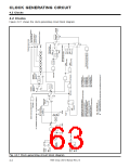
CLOCK GENERATING CIRCUIT
4.2 Clocks
(3) System clock select bit (bit 5)
This bit selects a clock source of fsys. When this bit = “0,” fXIN is selected as fsys; and when this bit =
“1,” fPLL as the one. (See Table 4.2.1.)
Clearing the PLL circuit operation enable bit (bit 1) to “0” clears the system clock select bit to “0.” Also,
while the PLL circuit operation enable bit = “0,” nothing can be written to the system clock select bit.
(Fixed to be “0.”)
In order to set the system clock select bit to “1” after reset, it is necessary to wait 2 ms after the
stabilization of f(XIN).
To rewrite the PLL multiplication ratio select bits (bits 2 and 3), clear the system clock select bit to
“0” simultaneously. Then, set this bit to “1” 2 ms after the rewriting of the PLL multiplication ratio select
bits. (See Figure 4.2.3.)
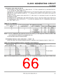
Table 4.2.1 fsys selection
fsys
Clock source
PLL circuit operation PLL multiplication ratio select bits
System clock select bit
(bit 5)
enable bit (bit 1)
(bits 3, 2) (Note 1)
Frequency (Note 2)
f(XIN)
–
0
1
–
fXIN
fPLL
fPLL
fPLL
01 (double)
10 (triple)
1
f(XIN) ❈ 2
f(XIN) ❈ 3
f(XIN) ❈ 4
11 (quadruple)
Notes 1: The PLL multiplication ratio select bits must be set so that fsys is in the range from 10 MHz to 20 MHz. After
reset, these bits are allowed to be changed only once.
2: Be sure that fsys does not exceed 20 MHz.
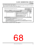
(4) Peripheral device’s clock select bits 1, 0 (bits 7, 6)
These bits select the internal peripheral device’s operation clock frequency listed in Table 4.2.2.
Table 4.2.2 Internal peripheral device’s operation clock frequency
Peripheral device’s clock select bits 1, 0
01
10
Internal peripheral
device’s operation clock
00
11
(Note)
f1
f2
fsys
fsys
fsys/2
fsys/2
fsys
fsys/4
f16
fsys/16
fsys/64
fsys/512
fsys/4096
fsys/8
fsys/32
Do not select.
f64
fsys/32
fsys/256
fsys/2048
fsys/128
fsys/1024
fsys/8192
f512
f4096
Note: To set the peripheral device’s clock select bits 1, 0 to “01 ,” be sure that a frequency of fsys must be 10 MHz or less.
2
7906 Group User’s Manual Rev.2.0
4-7

 RENESAS [ RENESAS TECHNOLOGY CORP ]