APPENDIX
Appendix 7. Countermeasure against noise
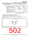
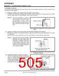
(3) Wiring for MD0 and MD1 pins
Connect MD0 and MD1 pins to the Vss pin (or Vcc pin) with the shortest possible wiring.
Reason: The processor mode of the
microcomputer is influenced by a
M37906
MD1
M37906
MD1
Noise
potential at the MD0 and MD1 pins
when the MD0 and MD1 pins and
the Vss pin (or Vcc pin) are
connected.
If the noise causes a potential
difference between the MD0 and
MD1 pins and the Vss pin (or Vcc
pin), the processor mode may
become unstable. This may cause
a microcomputer malfunction or
a program runaway.
MD0
Vss
MD0
Vss
Not Acceptable
Acceptable
Fig. 4 Wiring for MD0 and MD1 pins
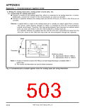
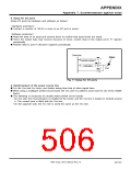
2. Connection of bypass capacitor between Vss and Vcc lines
Connect an approximate 0.1 µF bypass capacitor as follows:
ꢀ Connect a bypass capacitor between the Vss and Vcc pins, at equal lengths.
ꢀ The wiring connecting the bypass capacitor between the Vss and Vcc pins should be as short as
possible.
ꢀ Use thicker wiring for the Vss and Vcc lines than that for the other signal lines.
Bypass capacitor
Wiring pattern
Wiring pattern
Vcc
Vss
M37906
Fig. 5 Bypass capacitor between Vss and Vcc lines
7906 Group User’s Manual Rev.2.0
20-97

 RENESAS [ RENESAS TECHNOLOGY CORP ]