CENTRAL PROCESSING UNIT (CPU)
2.2 Bus interface unit (BIU)
2.2.2 Data Transfer (read and write)
When the CPU reads or writes data from or to the internal area, it requests the BIU to read or write data.
The BIU outputs control signals in order to control the internal address and data buses in response to the
request from the CPU. The cycle where the following are performed is referred to “bus cycle”:
• The BIU controls buses.
• Data transfer is performed between the internal area and BIU.
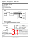
Table 2.2.4 lists the bus cycles at access to the internal area. Figure 2.2.4 shows operating waveform
examples at reading from or writing to the internal area.
(1) Reading data
The CPU informs the BIU’s data address register of the address where the data to be read is stored,
so the CPU requests the data. In this case, the CPU waits until the requested data is ready in the
BIU.
The BIU outputs the address informed by the CPU onto the internal address bus. Then, the CPU
reads the contents of the informed address and takes them into the data buffer. The CPU continues
processing using data in the data buffer.
(2) Writing data
The CPU informs the BIU’s data address register of the address to which the data will be written,
so the CPU writes the data into the data buffer. The BIU outputs the address informed by the CPU
onto the internal address bus. Then, the BIU writes the data in the data buffer into the informed
address.
Table 2.2.4 Bus cycles at access to internal area
Bus cycle = 3φ (Note)
Bus cycle = 2φ (Note)
(Internal ROM bus cycle select bit = 0)
(Internal ROM bus cycle select bit = 1)
1 bus cycle = 2φ
1 bus cycle = 3φ
φBIU
φBIU
ROM
Internal address bus
Internal data bus
Internal address bus
Internal data bus
Address
Address
Data
Data
1 bus cycle = 2φ
RAM
SFR
φ
BIU
Internal address bus
Internal data bus
Address
Data
Internal ROM bus cycle select bit: Bit 7 at address 5F16
Note: We usually recommend to select “bus cycle = 2 φ.” When reprogramming the internal flash memory
in the CPU reprogramming mode, be sure to select bus cycle = 3φ. (Refer to section “19.2 Flash
memory CPU reprogramming mode.”)
7906 Group User’s Manual Rev.2.0
2-12

 RENESAS [ RENESAS TECHNOLOGY CORP ]