INPUT/OUTPUT PINS
5.2 Programmable I/O ports
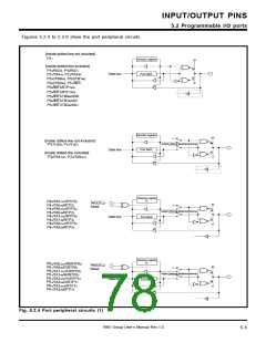
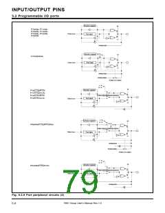
Figures 5.2.4 to 5.2.6 show the port peripheral circuits.
[Inside dotted-line not included]
P2
7
Direction register
Port latch
[Inside dotted-line included]
P1
P2
2/R
X
D
0
, P1
6
/R
/TA9IN
(/TB1IN
/INT
X
D
1
Data bus
1/TA4IN, P2
3
P2
P2
P5
P5
P5
P5
P5
4
6
2
3
5
6
7
(/TB0IN), P2
(/TB2IN), P5
5
)
1
1
/INT
/INT
/INT
/INT
/INT
2
3
5
6
7
/RTPTRG1
/RTPTRG0
/TB0IN/IDW
/TB1IN/IDV
/TB2IN/IDU
Direction register
Port latch
1
[Inside dotted-line not included]
P1
Output (internal peripheral device)
3
/TX
D0
, P1
7
/T
X
D1
Data bus
[Inside dotted-line included]
P20
/TA4OUT, P2 /TA9OUT
2
Direction register
R
P4
P4
P4
P4
P4
P4
P4
P4
0
1
2
3
4
5
6
7
/TA5OUT/RTP2
/TA5IN/RTP2
/TA6OUT/RTP2
/TA6IN/RTP2
/TA7OUT/RTP3
/TA7IN/RTP3
/TA8OUT/RTP3
/TA8IN/RTP3
0
2
0
2
P4OUTCUT
Reset
1
1
Output (internal peripheral device)
3
Data bus
Port latch
1
3
Direction register
R
P60
P61
P62
P63
P64
P65
P66
P67
/TA0OUT/W/RTP0
/TA0IN/V/RTP0
/TA1OUT/U/RTP0
/TA1IN/W/RTP0
/TA2OUT/V/RTP1
/TA2IN/U/RTP1
/TA3OUT/RTP1
/TA3IN/RTP1
0
P6OUTCUT
Reset
1
1
2
Output (internal peripheral device)
3
0
Port latch
Data bus
1
2
3
Fig. 5.2.4 Port peripheral circuits (1)
7905 Group User’s Manual Rev.1.0
5-5

 RENESAS [ RENESAS TECHNOLOGY CORP ]