INPUT/OUTPUT PINS
5.3 Examples of handling unused pins
5.3 Examples of handling unused pins
When unusing an I/O pin, some handling is necessary for this pin. Examples of handling unused pins are
described below.
The following are just examples. In actual use, the user shall modify them according to the user’s application
and properly evaluate their performance.
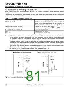
Table 5.3.1 Example of handling unused pins
Pin name
Handling example
P1, P2, P4 to P8
Set these pins to the input mode and connect each
pin to Vcc or Vss via a resistor; or set these pins to
the output mode and leave them open (Note 1).
Connect this pin to Vcc via a resistor.
P4OUTCUT/INT0, P6OUTCUT/INT
4
Select a falling edge for pins INT
Leave these pins open.
0
and INT .
4
X
OUT (Note 2), VCONT (Note 3)
Connect this pin to Vcc.
AVCC
AVSS, VREF
Connect these pins to Vss.
Notes 1: When leaving these pins open after they have been set to the output mode, note the following:
these port pins are placed in the input mode from reset until they are switched to the output mode
by software. Therefore, voltage levels of these pins are undefined and the power source current
may increase while these port pins are placed in the input mode.
Software reliability can be enhanced by setting the contents of the above ports’ direction registers
periodically. This is because these contents may be changed by noise, a program runaway which
occurs owing to noise, etc.
For unused pins, use the shortest possible wiring (within 20 mm from the microcomputer’s pins).
2: This applies when a clock externally generated is input to pin XIN.
3: Be sure that the PLL circuit operation enable bit (bit 1 at address BC16) = “0.”
ꢀ When setting port pins to input mode
ꢀ When setting port pins to output mode
Left open
Left open
P1, P2, P4 to P8
P1, P2, P4 to P8
X
OUT
X
OUT
V
CONT
Left open
V
CONT
VCC
VCC
AVCC
AVSS
AVCC
AVSS
VREF
V
REF
VCC
V
CC
V
SS
P4OUTCUT/INT
0
P4OUTCUT/INT
0
P6OUTCUT/INT
4
P6OUTCUT/INT
4
V
SS
Fig. 5.3.1 Example of handling unused pins
7905 Group User’s Manual Rev.1.0
5-8

 RENESAS [ RENESAS TECHNOLOGY CORP ]