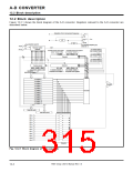
A-D CONVERTER
12.2 Block description
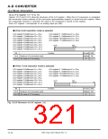
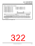
b7 b6 b5 b4 b3 b2 b1 b0
A-D control register 2 (Address DB16
)
0
0 0 0
Bit
0
Bit name
Function
At reset R/W
b3 b2 b1 b0
0
0
RW
RW
Analog input pin select bits 1
0 ❈❈❈ : Pins AN0 to AN7 are selected.
1 0 0 0 : Pin AN8 is selected.
1 0 0 1 : Pin AN9 is selected.
1 0 1 0 : Pin AN10 is selected.
1 0 1 1 : Pin AN11 is selected.
1 1 0 0 : Do not select.
(Note 2)
(Note 3)
(Note 4)
(Note 5)
(Note 6)
(Note 1)
1
2
RW
RW
RW
0
0
0
3
1 1 1 1 : Do not select.
7 to 4
Fix these bits to “0000.”
❈ : They may be either “0” or “1.”
Note 1: When using pins AN0 to AN7, regardless of the A-D operation mode, be sure to fix bit 3 to “0.” Also, pins AN8 to AN11 are
used only in the one-shot mode and repeat mode.
2: Select pins AN0 to AN7 at bits 2 to 0 of A-D control register 0 (address 1E16).
3: When using pin AN8, be sure that the D-A1 output enable bit (bit 1 at address 9616) = “0” (output disabled). Also, be sure not
to use pin CTS2/RTS2.
4: When using pin AN9, be sure not to use pin CTS2/CLK2.
5: When using pin AN10, be sure not to use pin RXD2.
6: When using pin AN11, be sure not to use pin TXD2.
7: Writing to each bit of A-D control register 2 must be performed while the A-D conversion halts, regardless of the A-D
operation mode.
Fig. 12.2.4 Structure of A-D control register 2
7905 Group User’s Manual Rev.1.0
12-7

 RENESAS [ RENESAS TECHNOLOGY CORP ]