A-D CONVERTER
12.2 Block description
12.2.1 A-D control registers 0, 1, and 2
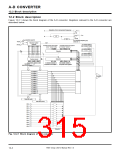
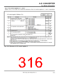
Figures 12.2.2, 12.2.3 and 12.2.4 show the structures of the A-D control registers 0, 1 and 2, respectively.
b7 b6 b5 b4 b3 b2 b1 b0
A-D control register 0 (Address 1E16)
0
Bit
0
Bit name
Function
At reset R/W
Undefined RW
b2 b1b0
Analog input pin select bits
0 0 0 : AN0 is selected.
0 0 1 : AN1 is selected.
0 1 0 : AN2 is selected.
0 1 1 : AN3 is selected.
1 0 0 : AN4 is selected.
1 0 1 : AN5 is selected.
1 1 0 : AN6 is selected.
1 1 1 : AN7 is selected.
(Valid in the one-shot and repeat
modes.)
(Note 1)
Undefined RW
Undefined RW
1
2
(Note 2)
b4 b3
0
0
RW
RW
3
4
A-D operation mode select bits 0
0 0 : One-shot mode
0 1 : Repeat mode
1 0 : Single sweep mode
1 1 : Repeat sweep mode 0 or 1
5
6
Fix this bit to “0.”
0
0
RW
RW
A-D conversion start bit
0 : A-D conversion halts.
1 : A-D conversion starts.
(Note 3)
RW
A-D conversion frequency (φAD)
select bit 0
7
See Table 12.2.1.
0
Notes 1: When using pins AN0 to AN7, be sure to fix bit 3 of the analog input pin select bits 1 (bits 3 to 0 at address DB16) to “0.”
Setting bit 3 of the analog input pin select bits 1 to “1” invalidates these bits.
Also, these bits are invalid in the single sweep mode, repeat sweep mode 0 and repeat sweet mode 1. (Each may be
either “0” or “1.”)
2: When using pin AN7, be sure that the D-A0 output enable bit (bit 0 at address 9616) = “0” (output disabled).
3: When writing to this bit, use the MOVM (MOVMB) or STA (STAB, STAD) instruction.
4: Writing to each bit (except writing of “0” to bit 6) of the A-D control register 0 must be performed while the A-D converter
halts, regardless of the A-D operation mode.
Fig. 12.2.2 Structure of A-D control register 0
7905 Group User’s Manual Rev.1.0
12-5

 RENESAS [ RENESAS TECHNOLOGY CORP ]