SERIAL I/O
11.3 Clock synchronous serial I/O mode
(2) Input of transfer clock from the external
A clock input from the CLK pin becomes the transfer clock.
i
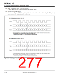
(3) Porarity of transfer clock
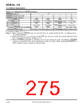
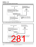
As shown in Figure 11.3.1, the polarity of the transfer clock can be selected by the CLK polarity
select bit (bit 6 at addresses 3416, 3C166, B416).
ꢀ CLK polarity select bit = 0
CLK
i
D0
D0
D1
D1
D2
D2
D3
D3
D4
D4
D5
D5
D6
D6
D7
D7
TxD
i
RxD
i
ꢀThe transmit data is output to the TxDi pin at the falling edge of a transfer clock, and the receive data is
input from the RxDi pin at the rising edge of the transfer clock.
The level at the CLKi pin is “H” when the transfer is not performed.
ꢀ CLK polarity select bit = 1
CLK
i
D0
D0
D1
D1
D2
D2
D3
D3
D4
D4
D5
D5
D6
D6
D7
D7
TxD
i
RxD
i
ꢀThe transmit data is output to the TxDi pin at the rising edge of a transfer clock, and the receive data is
input from the RxDi pin at the falling edge of the transfer clock.
The level at the CLKi pin is “L” when the transfer is not performed.
Fig. 11.3.1 Polarity of transfer clock
7905 Group User’s Manual Rev.1.0
11-22

 RENESAS [ RENESAS TECHNOLOGY CORP ]