SERIAL I/O
11.2 Block description
11.2.9 Port P1 direction register, Port P8 direction register
I/O pins for serial I/O are multiplexed with port P1 and P8 pins. When using pins P1
1
, P1
2
, P1
5
, P1
6
, P8 ,
1
and P8
direction registers to “0” in order to set these pins for the input mode. When using these pins as other serial
I/O’s pins (CTS /RTS , CLK , TxD ), these pins are forcibly set as I/O pins for serial I/O regardless of the
2
as serial I/O’s input pins (CTS
i
, RxD
i
), clear the corresponding bits of the port P1 and port P8
i
i
i
i
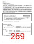
port P1 and port P8 direction registers’ contents. Figure 11.2.14 shows the relationship between the port
P1 and port P8 direction registers and serial I/O’s I/O pins. For details, refer to the description of each
operating mode.
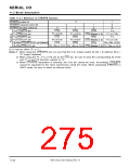
b7 b6 b5 b4 b3 b2 b1 b0
Port P1 direction register (Address
516)
Bit
0
Corresponding pin name
Function
At reset
R/W
RW
RW
RW
RW
RW
RW
RW
RW
Pin CTS0/RTS0
Pin CTS0/CLK0
Pin RxD0
0
0
0
0
0
0
0
0
0 : Input mode
1 : Output mode
1
2
When using pins P11, P12, P15, and P16 as serial
I/O’s input pins (CTS0, RxD0, CTS1, RxD1), clear
the corresponding bits to “0.”
3
Pin TxD0
4
Pin CTS1/RTS1
Pin CTS1/CLK1
Pin RxD1
5
6
7
Pin TxD1
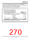
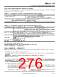
b7 b6 b5 b4 b3 b2 b1 b0
Port P8 direction register (Address 1416
)
Bit
0
Corresponding pin name
Function
At reset
R/W
RW
Pin CTS2/RTS2 (Pin AN8/DA1)
0
0 : Input mode
1 : Output mode
(Note 1)
Pin CTS2/CLK2 (Pin AN9)
1
2
0
RW
RW
RW
–
When using pins P81 and P82 as serial I/O’s input
pins (CTS2, RxD2), clear the corresponding bits to
“0.”
Pin RxD2 (Pin AN10)
Pin TxD2 (Pin AN11)
Nothing is assigned.
0
0
3
7 to 4
Undefined
Notes 1: When using pin CTS2/RTS2, be sure that the D-A1 output enable bit (bit 1 at address 9616) = “0” (output disabled).
2: ( ) shows the I/O pins of other internal peripheral devices which are multiplexed.
Fig. 11.2.14 Relationship between port P1 and port P8 direction registers and serial I/O’s I/O pins
7905 Group User’s Manual Rev.1.0
11-18

 RENESAS [ RENESAS TECHNOLOGY CORP ]