SERIAL I/O
11.2 Block description
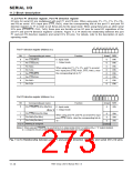
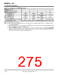
Table 11.2.1 Selection of CTS/RTS function
0
1
CTS/RTS enable bit
0
ꢀ
ꢀ
CTSi/RTSi separate select bit
1
ꢀ
0
1
CTS/RTS function select bit
CTS0
RTS0
P11 or CLK0
RTS1
P10
P10/CTS0/RTS0 pin
RTS0
P11 or CLK0
CTS1
P11/CTS0/CLK0 pin
P11 or CLK0
P14
CTS0 (Notes 2, 3)
RTS1
P14/CTS1/RTS1 pin
P15 or CLK1
CTS2
P15/CTS1/CLK1 pin
P15 or CLK1
RTS2
P15 or CLK1
P80, AN8, or DA1
P81, AN9, or CLK2
CTS1 (Notes 2, 3)
RTS2
P80/AN8/CTS2/RTS2/DA1 pin (Note1)
P81/AN9/CTS2/CLK2 pin
P81, AN9 or CLK2
P81, AN9 or CLK2
CTS2 (Notes 2, 3)
ꢀ: It may be either “0” or “1.”
Notes 1: When using the CTS2/RTS2 pin, be sure that the D-A1 output enable bit (bit 1 at address 9616) =
“0” (output disabled).
2: When using the P1
port P1 or port P8 direction register to “0.”
3: When CTS /RTS separation is selected, the CLK
1
, P1
5
, or P8
1
pin as the CTS pin, be sure to clear the corresponding bit of the
i
i
i
i
pin cannot be used. Accordingly, CTS
i
/RTS
i
cannot be separated in the clock synchronous serial I/O mode. When separating CTS
UART mode, be sure to select an internal clock.
i
/RTS in
i
7905 Group User’s Manual Rev.1.0
11-20

 RENESAS [ RENESAS TECHNOLOGY CORP ]