SERIAL I/O
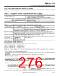
11.3 Clock synchronous serial I/O mode
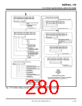
UART0 transmit/receive mode register (Address 3016
UART1 transmit/receive mode register (Address 3816
UART2 transmit/receive mode register (Address B016
)
)
)
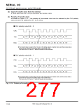
When external clock is selected
When internal clock is selected
b7
b0
UART0 baud rate register (BRG0) (Address 3116
UART1 baud rate register (BRG1) (Address 3916
UART2 baud rate register (BRG2) (Address B116
)
)
)
ꢀ
0
ꢀ
0
0
1
ꢀ
Selection of clock synchronous serial
I/O mode
b7 b0
Internal/External clock select bit
0: Internal clock
1: External clock
ꢀ: It may be either “0” or “1.”
Can be set to “0016” to “FF16.”
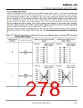
UART0 transmit/receive control register 0 (Address 3416
)
UART1 transmit/receive control register 0 (Address 3C16
)
UART0 transmit interrupt control register (Address 7116
UART1 transmit interrupt control register (Address 7316
)
)
UART2 transmit/receive control register 0 (Address B416
)
UART2 transmit interrupt control register (Address F116
b7 b0
)
b7 b0
BRG count source select bits
b1 b0
Interrupt priority level select bits
When using interrupts, set these bits to
one of levels 1 to 7.
When disabling interrupts, set these bits
to level 0.
0 0: f
2
0 1: f16
1 0: f64
1 1: f512
CTS/RTS function select bit
0: CTS function selected
1: RTS function selected
UART0 transmit buffer register (Address 3216
)
UART1 transmit buffer register (Address 3A16
UART2 transmit buffer register (Address B216
)
)
CTS/RTS enable bit
0: CTS/RTS function is enabled.
1: CTS/RTS function is disabled.
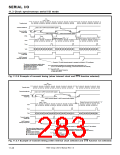
b7
b0
CLK polarity select bit
0: At the falling edge of the transfer
clock, transmit data is output
1: At the rising edge of the transfer
clock, transmit data is output
Transmit data is set.
Transfer format select bit
0: LSB first
1: MSB first
UART0 transmit/receive control register 1 (Address 3516
UART1 transmit/receive control register 1 (Address 3D16
UART2 transmit/receive control register 1 (Address B516
)
)
)
b7
b0
Serial I/O pin control register (Addre
1
s
6
s AC16
)
1
b7 b0
Transmit enable bit
1: Transmission is enabled.
CTS0/RTS
0
separate select bit
0: CTS
0
/RTS
separate select bit
are used together (Note)
0 are used together (Note)
CTS /RTS
0: CTS /RTS
TxD /P1 switch bit
0: Functions as TxD0.
TxD /P1 switch bit
0: Functions as TxD1.
CTS /RTS separate select bit
0: CTS /RTS are used together (Note)
TxD /P8 switch bit
1
1
1
1
0
3
1
7
2
2
2
2
Transmission starts.
2
3
0: Functions as TxD2.
(In the case of selecting the CTS function, transmission
starts when the CTS pin’s input level is “L.”)
0
Note: In the clock synchronous serial I/O
mode, CTSi/RTSi separation cannot
be selected. (Refer to section “[Pre-
cautions for clock synchronous
serial I/O mode].”)
Fig. 11.3.2 Initial setting example for relevant registers when transmitting
7905 Group User’s Manual Rev.1.0
11-25

 RENESAS [ RENESAS TECHNOLOGY CORP ]