SERIAL I/O
11.2 Block description
11.2.8 Serial I/O pin control register
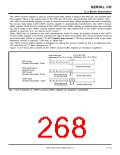
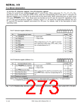
Figure 11.2.13 shows the structure of the seral I/O pin control register.
b7 b6 b5 b4 b3 b2 b1 b0
At reset R/W
Serial I/O pin control register (Address AC16)
Bit
0
Bit name
Function
CTS0/RTS0 separate select bit
0 : CTS0/RTS0 are used together.
1 : CTS0/RTS0 are separated.
0
RW
(Note)
0 : CTS1/RTS1 are used together.
1 : CTS1/RTS1 are separated.
CTS1/RTS1 separate select bit
(Note)
1
0
RW
0 : Functions as TxD0.
1 : Functions as P13.
TxD0/P13 switch bit
2
3
4
0
0
0
RW
RW
0 : Functions as TxD1.
1 : Functions as P17.
TxD1/P17 switch bit
0 : CTS2/RTS2 are used together.
1 : CTS2/RTS2 are separated.
CTS2/RTS2 separate select bit
(Note)
RW
RW
0 : Functions as TxD2.
1 : Functions as P83.
5
TxD2/P83 switch bit
0
0
7, 6
The value is “00” at reading.
—
Note: Valid when the CTS/RTS enable bit (bit 4 at addresses 3416, 3C16, and B416) is “0.”
Fig. 11.2.13 Structure of serial I/O pin control register
(1) CTS
0
/RTS
0
separate select bit (bit 0)
Refer to section “11.2.10 CTS/RTS function.”
(2) CTS
1
/RTS
1
separate select bit (bit 1)
Refer to section “11.2.10 CTS/RTS function.”
(3) TxD
0
/P1
3
switch bit (bit 2)
When this bit is set to “1,” the TxD
0
pin functions as a programmable I/O port pin (P1
3
). When only
reception is performed, the TxD
0
pin can be used as the P1 pin. When performing transmission, be
3
sure to clear this bit to “0.”
(4) TxD
1
/P1
7
switch bit (bit 3)
When this bit is set to “1,” the TxD
1
pin functions as a programmable I/O port pin (P1
7
). When only
reception is performed, the TxD
1
pin can be used as the P1 pin. When preforming transmission, be
7
sure to clear this bit to “0.”
(5) CTS
2
/RTS
2
separate select bit (bit 4)
Refer to section “11.2.10 CTS/RTS function.”
(6) TxD
2
/P8
3
switch bit (bit 5)
When this bit is set to “1,” the TxD
2
pin functions as a programmable I/O port pin (P8
3
). When only
reception is performed, the TxD
2
pin can be used as the P8 pin. When preforming transmission, be
3
sure to clear this bit to “0.”
7905 Group User’s Manual Rev.1.0
11-17

 RENESAS [ RENESAS TECHNOLOGY CORP ]