TIMER A
7.4 Event counter mode
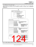
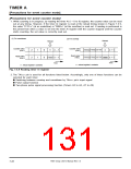
b7 b6 b5 b4 b3 b2 b1 b0
At reset R/W
Up-down register 0 (Address 4416
)
Function
Bit
0
Bit name
0 : Countdown
1 : Countup
Timer A0 up-down bit
0
0
0
0
0
0
RW
RW
RW
RW
RW
Timer A1 up-down bit
Timer A2 up-down bit
Timer A3 up-down bit
Timer A4 up-down bit
1
This function is valid when the contents of the up-
down register is selected as the up-down switching
factor.
2
3
4
Timer A2 two-phase pulse signal
processing select bit
0 : Two-phase pulse signal processing function disabled
1 : Two-phase pulse signal processing function enabled
5
WO
(Note)
Timer A3 two-phase pulse signal
processing select bit
0
0
WO
(Note)
6
7
When not using the two-phase pulse signal processing
function, clear the bit to “0.”
The value is “0” at reading.
Timer A4 two-phase pulse signal
processing select bit
WO
(Note)
Note: Use the MOVM (MOVMB) or STA(STAB, STAD) instruction for writing to bits 5 to 7.
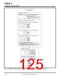
b7 b6 b5 b4 b3 b2 b1 b0
Up-down register 1 (Address C416
)
Function
Bit
0
Bit name
At reset R/W
0 : Countdown
1 : Countup
Timer A5 up-down bit
0
0
0
0
0
0
RW
RW
RW
RW
RW
Timer A6 up-down bit
Timer A7 up-down bit
Timer A8 up-down bit
Timer A9 up-down bit
1
This function is valid when the contents of the up-
down register is selected as the up-down switching
factor.
2
3
4
Timer A7 two-phase pulse signal
processing select bit
0 : Two-phase pulse signal processing function disabled
1 : Two-phase pulse signal processing function enabled
5
WO
(Note)
Timer A8 two-phase pulse signal
processing select bit
0
0
WO
(Note)
6
7
When not using the two-phase pulse signal processing
function, clear the bit to “0.”
The value is “0” at reading.
Timer A9 two-phase pulse signal
processing select bit
WO
(Note)
Note: Use the MOVM (MOVMB) or STA(STAB, STAD) instruction for writing to bits 5 to 7.
Fig. 7.4.5 Structures of up-down registers 0 and 1
7905 Group User’s Manual Rev.1.0
7-25

 RENESAS [ RENESAS TECHNOLOGY CORP ]