TIMER A
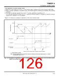
7.4 Event counter mode
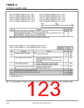
Timer A0 register (Addresses 4716, 4616)
Timer A1 register (Addresses 4916, 4816)
Timer A2 register (Addresses 4B16, 4A16)
Timer A3 register (Addresses 4D16, 4C16)
Timer A4 register (Addresses 4F16, 4E16)
Timer A5 register (Addresses C716, C616)
Timer A6 register (Addresses C916, C816)
Timer A7 register (Addresses CB16, CA16)
Timer A8 register (Addresses CD16, CC16)
Timer A9 register (Addresses CF16, CE16)
(b8)
b0 b7
(b15)
b7
b0
Bit
Function
Any value in the range from “000016” to “FFFF16” can be set.
At reset R/W
RW
15 to 0
Undefined
Assuming that the set value = n, the counter divides the count source frequency by (n + 1)
during countdown, or by (FFFF16 – n + 1) during countup.
When reading, the register indicates the counter value.
Note: Reading from or writing to this register must be performed in a unit of 16 bits.
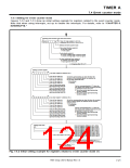
Timer Ai mode register (i = 0 to 4) (Addresses 5616 to 5A16)
b7 b6 b5 b4 b3 b2 b1 b0
Timer Ai mode register (i = 5 to 9) (Addresses D616 to DA16)
X X 0
0 1
Bit
0
Bit name
Function
0 1 : Event counter mode
At reset R/W
b1 b0
Operating mode select bits
0
0
0
RW
RW
RW
1
2
0 : No pulse output (TAiOUT pin functions as a
programmable I/O port pin.)
Pulse output function select bit
1 : Pulse output (TAiOUT pin functions as a pulse
output pin.)
0 : Counts at falling edge of external signal
1 : Counts at rising edge of external signal
Count polarity select bit
0
0
RW
RW
3
4
0 : Contents of up-down register
1 : Input signal to TAiOUT pin
Up-down switching factor select
bit
0
0
0
RW
RW
RW
Fix this bit to “0” in event counter mode.
5
6
7
These bits are invalid in event counter mode.
X : It may be either “0” or “1.”
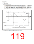
Fig. 7.4.1 Structures of timer Ai register and timer Ai mode register in event counter mode
7905 Group User’s Manual Rev.1.0
7-20

 RENESAS [ RENESAS TECHNOLOGY CORP ]