TIMER A
7.2 Block description
7.2.6 Port P2, port P4 and port P6 direction registers
The I/O pins of timers A0 to A3 are multiplexed with port P6 pins, and the I/O pins of timers A4 and A9
are multiplexed with port P2 pins, and the I/O pins of timers A5 to A8 are multiplexed with port P4 pins.
When using these pins as timer Ai (i = 0 to 9)’s input pins, clear the corresponding bits of the port P6, port
P2, and port P4 direction registers to “0” in order to set these port pins for the input mode. When used
as timer Ai’s output pins, these pins are forcibly set to the output pins of timer Ai regardless of the direction
registers’ contents. Figure 7.2.6 shows the relationship between the port P6 direction register and the timer
Ai’s I/O pins, Figure 7.2.7 shows the relationship between port P2 and port P4 direction registers and timer
Ai’s I/O pins.
Note that each bit of the port P4 direction register becomes “0” by an input of a falling edge to pin
P4OUTCUT. (Refer to section “5.2.3 Pin P4OUTCUT/INT .”) When switching the output pins of timers A5 to
0
A8 to the port output pins, the following procedure is required.
➀ Return the input level at pin P4OUTCUT to “H.”
➀ Write data to the port P4 register’s bit corresponding to the port P4 pin, where data is to be output.
➀ Set “1” to the port P4 direction register’s bit corresponding to the above P4 register’s bit; therefore, this
bit enters the output mode.
When the input level at pin P4OUTCUT = “L,” no bit of the port P4 direction register can be set to “1.”
Similarly, each bit of the port P6 direction register becomes “0” by an input of a falling edge to pin
P6OUTCUT. (Refer to section “5.2.4 Pin P6OUTCUT/INT .”) When switching the output pins of timers A0 to
4
A3 to the port output pins, the following procedure is required.
➀ Return the input level at pin P6OUTCUT to “H.”
➀ Write data to the port P6 register’s bit corresponding to the port P6 pin, where data is to be output.
➀ Set “1” to the port P6 direction register’s bit corresponding to the above P6 register’s bit; therefore, this
bit enters the output mode.
When the input level at pin P6OUTCUT = “L,” no bit of the port P6 direction register can be set to “1.”
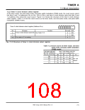
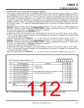
b7 b6 b5 b4 b3 b2 b1 b0
Port P6 direction register (Address 1016
)
Bit
0
Corresponding pin
Pin TA0OUT (Pin W/RTP00)
Pin TA0IN (Pin V/RTP01)
Pin TA1OUT (Pin U/RTP02)
Pin TA1IN (Pin W/RTP03)
Pin TA2OUT (Pin V/RTP10)
Pin TA2IN (Pin U/RTP11)
Pin TA3OUT (Pin RTP12)
Pin TA3IN (Pin RTP13)
Functions
At reset R/W
RW
RW
RW
RW
RW
RW
RW
RW
0
0
0
0
0
0
0
0 : Input mode
1 : Output mode
1
2
When using this pin as timer Ai’s input pin, be sure
to clear the corresponding bit to “0.”
3
4
5
6
7
0
Notes 1: Each of bits 0 to 7 becomes “0” by an input of the falling edge to pin P6OUTCUT/INT4. (Refer to section “5.2.4 Pin P6OUTCUT/
INT .”)
4
2: The pins in ( ) are I/O pins of other internal peripheral devices, which are multiplexed.
Fig. 7.2.6 Relationship between port P6 direction register and timer Ai’s I/O pins
7905 Group User’s Manual Rev.1.0
7-9

 RENESAS [ RENESAS TECHNOLOGY CORP ]