TIMER A
7.2 Block description
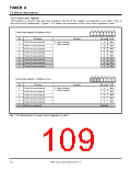
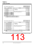
b7 b6 b5 b4 b3 b2 b1 b0
At reset R/W
Port P2 direction register (Address 816
)
Bit
0
Corresponding pin
Functions
0
0
0
0
0
0
0
0
RW
RW
RW
RW
RW
RW
RW
RW
Pin TA4OUT
0 : Input mode
1
1 : Output mode
Pin TA4IN
Pin TA9OUT
Pin TA9IN
Pin TB0IN
Pin TB1IN
Pin TB2IN
Pin P27
2
When using this pin as timer Ai’s input pin, be sure
to clear the corresponding bit to “0.”
3
4
(Note 1)
(Note 2)
(Note 3)
5
6
7
Notes 1: This applies when the TB0IN pin select bit (bit 0 at address AE16) = 1.
2: This applies when the TB1IN pin select bit (bit 1 at address AE16) = 1.
3: This applies when the TB2IN pin select bit (bit 2 at address AE16) = 1.
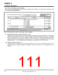
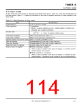
b7 b6 b5 b4 b3 b2 b1 b0
At reset R/W
Port P4 direction register (Address C16
)
Bit
0
Corresponding pin
Pin TA5OUT (Pin RTP20)
Pin TA5IN (Pin RTP21)
Pin TA6OUT (Pin RTP22)
Pin TA6IN (Pin RTP23)
Pin TA7IN (Pin RTP30)
Pin TA7IN (Pin RTP31)
Pin TA8OUT (Pin RTP32)
Pin TA8IN (Pin RTP33)
Functions
0
0
0
0
0
0
0
0
RW
RW
RW
RW
RW
RW
RW
RW
0 : Input mode
1
1 : Output mode
2
When using this pin as timer Ai’s input pin, be sure
to clear the corresponding bit to “0.”
3
4
5
6
7
Notes 1: Each of bits 0 to 7 becomes “0” by an input of the falling edge to pin P4OUTCUT/INT
INT .”)
2: The pins in ( ) are I/O pins of other internal peripheral devices, which are multiplexed.
0. (Refer to section “5.2.3 Pin P4OUTCUT/
0
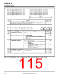
Fig. 7.2.7 Relationship between port P4 and port P2 direction registers and timer Ai’s I/O pins
7905 Group User’s Manual Rev.1.0
7-10

 RENESAS [ RENESAS TECHNOLOGY CORP ]