TIMER A
7.2 Block description
7.2.2 Timer A clock division select register
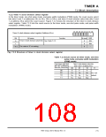
In the timer mode, one-shot pulse mode, and pulse width modulation (PWM) mode, the count source select
bits (bits 6 and 7 at addresses 5616 to 5A16, D616 to DA16), and timer A clock division select bits (bits 0 and
1 at address 4516) select the count source. Figure 7.2.2 shows the structure of the timer A clock division
select register. Table 7.2.3 lists the count source (in the timer mode, one-shot pulse mode, and pulse width
modulation (PWM) mode).
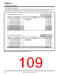
b7 b6 b5 b4 b3 b2 b1 b0
Timer A clock division select register (Address 4516)
Bit
0
Bit name
Function
At reset R/W
Timer A clock division select bits
See Table 7.2.3.
0
0
0
RW
RW
–
1
The value is “0” at reading.
7 to 2
Fig. 7.2.2 Structure of timer A clock division select register
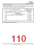
Table 7.2.3Count source (in timer mode, one-shot
pulse mode, and pulse width modulation
(PWM) mode)
Timer A clock division select bits
(bits 0 and 1 at address 4516
Count source select bits
(bits 6 and 7 at addresses
)
5616 to 5A16, D616 to DA16
)
00
01
10
11
00
01
10
11
f
2
f
1
f
1
f
f
16
f
f
16
f
64
512
4096
Do not
select.
64
64
f
f
512
f
4096
f
7905 Group User’s Manual Rev.1.0
7-5

 RENESAS [ RENESAS TECHNOLOGY CORP ]