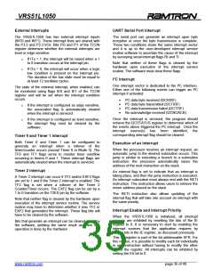
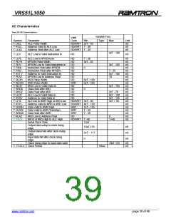
VRS51L1050
AC Characteristics
TABLE 53: AC CHARACTERISTICS
Variable Fosc
Valid
Symbol
T LHLL
T AVLL
T LLAX
Parameter
ALE Pulse Width
Address Valid to ALE Low
Address Hold after ALE Low
Cycle
Unit
nS
nS
Min.
Type
Max.
RD/WRT 2xT - 40
RD/WRT T - 40
RD/WRT T - 30
nS
4xT - 100
3xT -105
T LLIV
ALE Low to Valid Instruction In
RD
nS
T LLPL
T PLPH
T PLIV
T PXIX
T PXIZ
ALE Low to #PSEN low
#PSEN Pulse Width
RD
RD
RD
RD
RD
RD
RD
RD
WRT
RD
RD
RD
RD
RD
T - 30
3xT - 45
nS
nS
nS
nS
nS
nS
nS
nS
nS
nS
nS
nS
nS
nS
nS
nS
nS
nS
nS
nS
nS
#PSEN Low to Valid Instruction In
Instruction Hold after #PSEN
Instruction Float after #PSEN
Address to Valid Instruction In
#PSEN Low to Address Float
#RD Pulse Width
#WR Pulse Width
#RD Low to Valid Data In
Data Hold after #RD
0
T - 25
5xT - 105
10
T AVI V
T PLAZ
T RLRH
T WLWH
T RLDV
T RHDX
T RHDZ
T LLDV
T AVDV
T LLYL
T AVYL
T QVWH
T QVWX
T WHQX
T RLAZ
T YALH
6xT - 100
6xT - 100
5xT - 165
0
Data Float after #RD
2xT - 70
8xT - 150
9xT - 165
3xT + 50
ALE Low to Valid Data In
Address to Valid Data In
ALE low to #WR High or #RD Low
Address Valid to #WR or #RD Low
Data Valid to #WR High
Data Valid to #WR Transition
Data Hold after #WR
#RD Low to Address Float
#W R or #RD High to ALE High
Serial Clock Time
RD/WRT 3xT - 50
RD/WRT 4xT - 130
WRT
WRT
WRT
RD
7xT - 150
T - 50
T - 50
0
RD/WRT T -40
12xT
T+40
Output data setup to clock rising
edge
Output data hold after clock rising
edge
Input data hld after clock rising
edge
10xT-133
nS
nS
nS
2xT – 117
0
Clock rising edge to input data valid
T,TCLCL Clock Period
10xT-133
nS
nS
1/fosc
______________________________________________________________________________________________
www.ramtron.com page 39 of 49

 RAMTRON [ RAMTRON INTERNATIONAL CORPORATION ]