VRS51C1000
point anywhere in the 00h to FFh range of SRAM
memory. When a function call is performed or an
interrupt is serviced, the 16-bit return address (two
bytes) is stored on the stack. Data can be placed
manually on the Stack by using the PUSH and POP
functions.
Example:
Suppose that RAMS1, RAMS0 are set to 0 and
respectively and Rn has a value of 45h.
1
Performing MOVX @Rn, A, (where n is 0 or 1) allows the
user to transfer the value of A to the expanded SRAM at
address 145h (page 1).
Expanded SRAM Access Using the MOVX @DPTR
Instruction (0000-02FF, Bank4-Bank15)
Note that when both RAM1 and RAM0 are set to 1, the
value of P2 defines the upper byte and Rn defines the
lower byte of the external address. In this case the
device will access off-chip memory in the external
memory space using the external memory control
signals, Off chip peripherals can therefore be mapped
into the “P2value”00h to “P2value”FFh address range
The 768 bytes of the expanded SRAM data memory
occupies addresses 0000h to 02FFh. This can be
accessed using external direct addressing (i.e. using
the MOVX instruction) or by using bank mapping direct
addressing.
Note that in the case of indirect
addressing using the MOVX @DPTR instruction, if the
address is larger than 02FFh, the VRS51C1000 will
access off-chip memory in the external memory space
using the external memory control signals
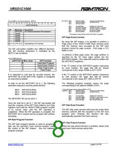
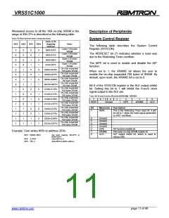
Data Bank Control Register
The DBANK register allows the user to enable the
Data Bank Select function and map the entire contents
of the SRAM memory in the range of 40h to 7Fh for
applications that would require direct addressing of the
expanded SRAM.
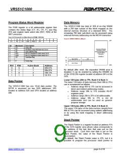
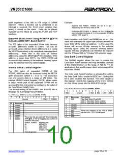
Internal SRAM Control Register
The 768 bytes of expanded SRAM of the
VRS51C1000 can also be accessed using the MOVX
@Rn instruction (where n = 0 or 1). This instruction
can only access data in a range of 256 bytes. The
internal SRAM Control Register, RCON, allows users
to select which part of the expanded SRAM will be
accessed by this instruction by configuring the value of
the RAMS0 and RAMS1 bits.
The Data Bank Select function is activated by setting
the Data Bank Select enable bit (BSE) to 1. Setting this
bit to zero disables this function. The lower nibble of
this register controls the mapping of the entire 1K byte
on-chip SRAM space into the 040h-07Fh range.
TABLE 14: DATA BANK CONTROL REGISTER (DBANK) – SFR 86H
The default setting of the RAMS1 and RAMS0 bits is
00 (page 0). Each page has 256 bytes.
7
6
5
4
3
2
1
0
BSE
Unused
BS3
BS2
BS1
BS0
TABLE 13: INTERNAL SRAM CONTROL REGISTER (RCON) - SFR 85H
7
6
5
4
3
2
1
0
Bit
Mnemonic Description
Unused
RAMS1
RAMS0
7
BSE
Data Bank Select Enable Bit
BSE=1, Data Bank Select enabled
BSE=0, Data Bank Select disabled
Bit
7
6
5
4
3
2
1
0
Mnemonic Description
6
5
4
3
2
1
0
Unused
Unused
Unused
BS3
BS2
BS1
-
-
-
Unused
Unused
Unused
Unused
Unused
Unused
RAMS1
RAMS0
-
-
-
-
-
-
Allows the mapping of the 1KB of SRAM
into the 040h - 07Fh SRAM space
BS0
These two bits are used with Rn of instruction
OVX @Rn, n=1,0 for mapping (see section on
extended 768 bytes)
RAMS1, RAMS0
00
01
10
Mapped area
000h-0FFh
100h-1FFh
200h-2FFh
XY00h-XYFF*
11
*Externally generated
______________________________________________________________________________________________
www.ramtron.com page 10 of 48

 RAMTRON [ RAMTRON INTERNATIONAL CORPORATION ]