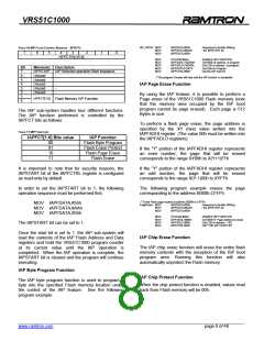
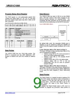
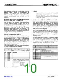
VRS51C1000
Power Control Register
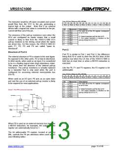
Input/Output Ports
The VRS51C1000 provides two power saving modes,
Idle and Power Down, which are controlled by the
PDOWN and IDLE bits of the PCON register at
address 87h.
The VRS51C1000 has 36 bi-directional lines grouped
into four 8-bit I/O ports and one 4-bit I/O port. These
I/Os can be individually configured as input or output.
Except for the P0 I/Os, which are of the open drain
type, each I/O is made of a transistor connected to
ground and a weak pull-up resistor (transistor based).
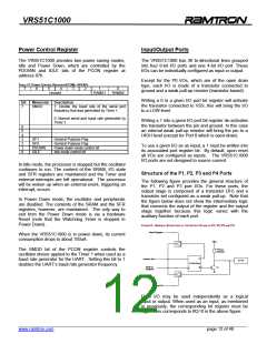
TABLE 17: POWER CONTROL REGISTER (PCON) - SFR 87H
7
6
5
4
3
2
1
0
Unused
RAMS1
RAMS0
Writing a 0 in a given I/O port bit register will activate
the transistor connected to VSS, this will bring the I/O
to a LOW level.
Bit
7
Mnemonic Description
SMOD
1: Double the baud rate of the serial port
frequency that was generated by Timer 1.
0: Normal serial port baud rate generated by
Timer 1.
Writing a 1 into a given I/O port bit register de-activates
the transistor between the pin and ground. In this case
an internal weak pull-up resistor will bring the pin to a
HIGH level (except for Port 0 which is open-drain).
6
5
4
3
2
1
0
GF1
GF0
PDOWN
IDLE
General Purpose Flag
General Purpose Flag
Power down mode control bit
Idle mode control bit
To use a given I/O as an input, a 1 must be written into
its associated port register bit. By default, upon reset
all I/Os are configured as inputs. The VRS51C1000
I/O ports are not designed to source current.
In Idle mode, the processor is stopped but the oscillator
continues to run. The content of the SRAM, I/O state
and SFR registers are maintained and the Timer and
external interrupts are left operational. The processor
will be woken up when an external event, triggering an
interrupt, occurs.
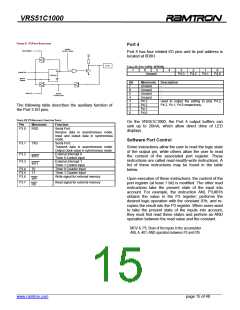
Structure of the P1, P2, P3 and P4 Ports
The following figure provides the general structure of
the P1, P2 and P3 port I/Os. For these ports, the
output stage is composed of a transistor (X1) and a
transistor set configured as a weak pull-up. Note that
the figure below does not show the intermediary logic
that connects the output of the register and the output
stage together because this logic varies with the
auxiliary function of each port.
In Power Down mode, the oscillator and peripherals
are disabled. The contents of the SRAM and the SFR
registers, however, are maintained. The only way to
exit from the Power Down mode is via a hardware
Reset (note that the Watchdog Timer is stopped in
Power Down).
FIGURE 6: GENERAL STRUCTURE OF THE OUTPUT STAGE OF P1, P2, P3 AND P4
Read Register
When the VRS51C1000 is in power down, its current
consumption drops to about 150uA.
Vcc
Pull-up
Network
The SMOD bit of the PCON register controls the
oscillator divisor applied to the Timer 1 when used as a
baud rate generator for the UART. Setting this bit to 1
doubles the UART’s baud rate generator frequency.
Q
Internal Bus
IC Pin
D Flip-Flop
Write to
Register
X1
Q
Read Pin
Each I/O may be used independently as a logical
input or output. When used as an input, as mentioned
in previously, the corresponding bit register must be
high. This corresponds to #Q=0 in the above figure.
______________________________________________________________________________________________
www.ramtron.com page 12 of 48

 RAMTRON [ RAMTRON INTERNATIONAL CORPORATION ]