VRS51C1000
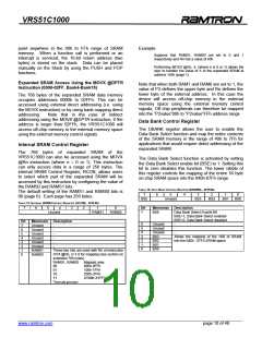
Windowed access to all the 1KB on-chip SRAM in the
range of 40h-7Fh is described in the following table.
Description of Peripherals
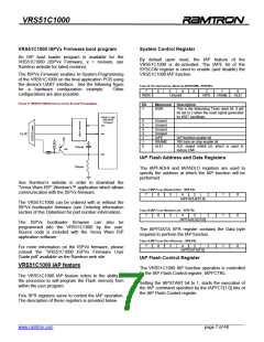
System Control Register
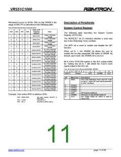
TABLE 15: BANK MAPPING DIRECT ADDRESSING MODE
040h~07fh
BS3
BS2
BS1
BSO
mapping
address
Note
The following table describes the System Control
Register (SYSCON).
Lower 128 bytes
SRAM
Lower 128 bytes
SRAM
Upper 128 bytes
SRAM
Upper 128 bytes
SRAM
0
0
0
0
0
0
0
0
1
1
1
1
1
1
1
1
0
0
0
0
1
1
1
1
0
0
0
0
1
1
1
1
0
0
1
1
0
0
1
1
0
0
1
1
0
0
1
1
0
1
0
1
0
1
0
1
0
1
0
1
0
1
0
1
000h-03Fh
040h-07Fh
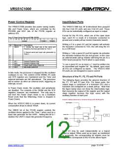
The WDRESET bit (7) indicates whether a reset was
due to the Watchdog Timer overflow.
080h-0BFh
The IAPE bit is used to enable and disable the IAP
function.
0C0h-0FFh
On-chip expanded
768 bytes SRAM
On-chip expanded
768 byte SRAM
On-chip expanded
768 byte SRAM
On-chip expanded
768 byte SRAM
On-chip expanded
768 bytes SRAM
On-chip expanded
768 bytes SRAM
On-chip expanded
768 bytes SRAM
On-chip expanded
768 bytes SRAM
On-chip expanded
768 bytes SRAM
On-chip expanded
768 bytes SRAM
On-chip expanded
768 bytes SRAM
On-chip expanded
768 bytes SRAM
0000h-003Fh
0040h-007Fh
0080h-00BFh
00C0h-00FFh
0100h-013Fh
0140h-017Fh
0180h-01BFh
01C0h-01FFh
0200h-023Fh
0240h-027Fh
0280h-02BFh
02C0h-02FFh
When set to 1, the XRAME bit allows the user to
enable the on-chip expanded 768 bytes of SRAM. By
default, upon reset, the XRAME bit is set to 0.
Bit 0 of the SYSCON register is the ALE output inhibit
bit. Setting this bit to 1 will inhibit the Fosc/6 clock
signal output to the ALE pin.
TABLE 16: SYSTEM CONTROL REGISTER (SYSCON) – SFR BFH
7
6
5
4
3
2
1
0
WDR
Unused
IAPE
XRAME
ALEI
Bit
Mnemonic Description
7
WDR
This is the Watchdog Timer reset bit. It will
be set to 1 when the reset signal generated
by WDT overflows.
6
5
4
3
2
1
0
Unused
Unused
Unused
Unused
IAPE
-
-
-
-
IAP function enable bit
Example: User writes #55h to address 203h:
XRAME
ALEI
768 bytes on-chip SRAM enable bit
ALE output inhibit bit, which is used to
reduce EMI.
MOV DBANK, #8CH
;Set bank mapping 40h-07Fh to
0200h-023Fh
;Store #55H to A
MOV A, #55H
MOV 43H, A
;Write #55H to 0203h ;address
______________________________________________________________________________________________
www.ramtron.com page 11 of 48

 RAMTRON [ RAMTRON INTERNATIONAL CORPORATION ]