4.2 SAMPLE CAPACITOR
4.5 AMPLIFIER
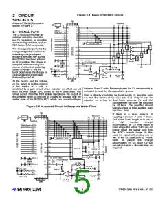
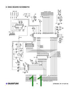
Charge sampler Cs should be a PPS film or NPO ceramic The amplifier chain should be as shown in the various figures
type for best stability. Acceptable Cs values range from 1nF in this datasheet. It should have 2 stages of gain, totaling
to 50nF. Lower values will increase circuit gain and hence about 100 +/-20%. Numerous opamps are available that will
key sensitivity; lower values also act to reduce the required perform to requirements, including the TI TLC2272 and the
burst length for a given desired sensitivity at the expense of Analog Devices OPA2340. The opamps should have at least
reduced inherent signal averaging.
a rail-to-rail CMOS output, and an input that can sense from
ground to at least +1 volt. The recommended GBW is 2MHz
or above. To reduce leakage current problems the amplifier
should be a JFET or CMOS input type only.
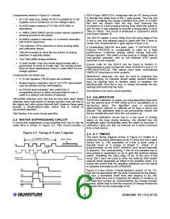
4.3 CZ CAPACITORS
The two Cz capacitors should have a value of 4% to 6% of
the total value of Cs + Cz1 + Cz2. The objective is to allow
the creation of a negative voltage step at Cs of about 0.25
volts with each Cz cap switched.
4.6 ESD PROTECTION
In general the QT60320D will be protected from direct static
discharge by the overlying panel. However, even with a
panel, transients can still flow into the electrode via induction,
or in extreme cases, via dielectric breakdown. Porous
materials may allow a spark to tunnel right through the
material. Testing is required to reveal any problems. The
QT60320D does have diode protection on its terminals which
In cases where the matrix is composed entirely of small keys,
the Cz caps may not actually fire, or perhaps only one of
them may fire. However, the device's error detection logic
requires the presence of these two capacitors in order to
function correctly.
If Cs = 15nF (a common value for the circuit), then each Cz can absorb and protect the device from most induced
should be 820pF. The Cz capacitors should be of type NPO discharges, up to 20mA; the usefulness of the internal
or C0G ceramic, or PPS film.
clamping will depending on the dielectric properties, panel
thickness, rise time of the ESD transients, and their duration.
4.4 R2R RESISTOR LADDER
The device pins can be further protected by inserting series
resistance into the X lines; similarly, the charge capture
circuitry (the PLD and analog switch) can similarly benefit
from series-R in the Y lines. The resistances chosen should
not be so high as to interfere with the QT process. Every
board layout is different and thus it is difficult to specify a
suitable value, however, typical values range from 200 ohms
to 10K ohms. In serious cases additional low-capacitance
high-conductance clamp diodes (e.g. BAV99) may be added
to shunt ESD aside.
The R2R resistor ladder network should be of value R=100K
ohms and have a precision of at least 7 bits. The nominal
resistance of the ladder is also the series impedance of the
ladder and affects the scaling of the offset injected into the
amplifier chain. The ladder should create an offset in the
output of the amplifier chain of about 0.15 volts / LSB. The
scaling of the offset injection also affects the crossover points
for the switching of each Cz capacitor. If during the
calibration cycle the R2R network is found to not provide
enough offset to bring the signal to the midpoint of the ADC's
range, a Cz capacitor will be switched in to create an
additional negative offset.
The QT60320's 'X' drive lines are always being driven at low
impedance; they are never 3-state unless the circuit is
powering up or is powered down. This is a considerable
advantage in dealing with ESD. The part's Y control pins do
not directly go to the matrix. The 4 user-input pins may be
vulnerable and should be resistor and/or diode protected if
they are in danger of being subject to ESD.
If the R2R value and Cz values are not properly matched, the
circuit may not be able to converge on a calibration point.
This will happen especially if the Cz cancellation voltage step
is too large.
LQ
9
QT60320D R1.11/12.07.03

 QUANTUM [ QUANTUM RESEARCH GROUP ]