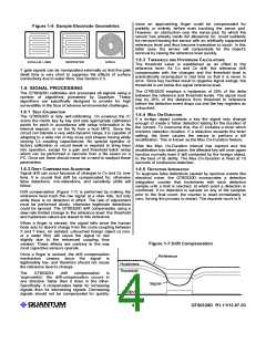
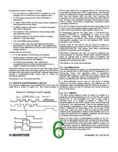
Components shown in Figure 2-1 include:
22V10 type CMOS PLD configured with an RC timing circuit
to shorten the dwell time of the Y gate pulses. This has the
effect of curtailing the charge collected from parts of a water
film that are distant from the key, thus reducing the
occurrence of cross-coupling among keys when the panel is
wet. Rt and Ct are adjusted to provide a timing delay of from
75ns to 100ns. This circuit is employed in Quantum's E6S3
eval board (Section 5).
ꢀ An LVD reset (e.g. Dallas DS1811) suitable for 5 volt
supplies and an active-low on low-voltage output;
ꢀ An R2R ladder network (CTS 750-107R100K or
equivalent);
ꢀ A >2MHz GBW CMOS rail-rail output opamp capable of
sensing ground on the inputs;
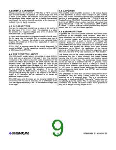
The 22V10 creates a short delay from the rising edge of the
X line in use; this delayed signal is gated with the Y lines to
create new, foreshortened Y-gate signals (Figure 2-3).
ꢀ An 8MHz crystal or resonator, or a ceramic resonator
with built-in capacitors;
ꢀ Two indicator LEDs (optional) to show sensing state
and calibration status;
A QualitySemi QS3125 'bus gate' (also: TI SN74CBT3125,
Pericom PI5C3125 or comparable) is used as a high
performance n-channel analog switch having near-zero
charge injection. The switch is only used as a charge drain to
near-ground potential, and so full bilateral 0-5V switch
operation is not required.
ꢀ 74AC04 inverters to drive the two banks of analog
switches in opposite states;
ꢀ Two 74HC4066 analog switches;
ꢀ A reset mosfet, most any small-signal mosfet with a
guaranteed on-state at 4 volts Vgs. The mosfet should
have an input capacitance (Ciss) of under 50pF for low
charge injection.
Source code for the 22V10 can be found in Section 5.
Representative parts include the Xilinx XCR22V10 and ICT's
PEEL22CV10AC-25. This device must have conventional
CMOS I/O structures to work properly.
Components not shown are:
Mechanical measures can also be used to suppress key
cross-coupling, for example raised plastic barriers between
keys (or placing keys in shallow wells) to lengthen the
electrical path from key to key, or simply increasing the key
spacing (and reducing key size).
ꢀ A +5 volt regulator (78L05 types are suitable);
ꢀ Supply bypass capacitors (two 0.1uF X7R caps placed
near the 60320 and the 74HC4066's);
ꢀ An RS232 level translator, like a MAX232 or
comparable device to allow communications over a
cable to a distant host device (if desired).
See Section 4 for more circuit specifics.
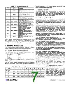
2.3 CALIBRATION
The 60320 calibrates on power-up using algorithms that seek
74HC4066 switches work fine but are less than ideal; these
switches have high levels of charge injection that will add to
the signal and also induce thermal drift. However these parts
provide a break-before-make action that is critical to
successful operation.
out the optimal level of R2R offset and Cz cancellation on a
successive
key-by-key basis. The algorithm uses
a
approximation method, to calibrate all 32 keys in about one
second. The calibration data is not permanently stored; the
device recalibrates each time the unit powers up.
See Section 4 for more circuit specifics.
If a false calibration occurs due to a key touch or foreign
object on the keys during powerup, the affected key will
2.2 WATER SUPPRESSING CIRCUIT
A circuit that suppresses cross-coupling from key to key by recalibrate again immediately when the object is removed. A
water films is shown in Figure 2-2. This circuit includes a calibration cycle can also be induced via a serial command
from a host device.
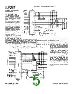
Figure 2-3 Timing of X and Y signals
2.4 X-Y TIMING
The basic timing diagram shown in Figure 2-3 relates to a
particular key being addressed by an XA drive line and a gate
control line YB. The acquisition of a key is done using a
'n' pulses / burst
R2R Value
Xa
discrete burst of X pulses of length 'n', where 'n' is
programmable via the UART interface (and stored internally
in eeprom). The corresponding Y line for the sampled key is
Yb
also pulsed in quadrature so as to gate the external analog
switch, straddling the rising edge of Xa. At the end of the
burst, the X pins are used to drive the external R2R ladder
Amp out
network which generates an offset to the amplifier chain. It is
during this period that the amplifier stabilizes and the signal
is sampled internally by the QT60320D.
Xa
Figure 2-3 also shows a dwell-adjusted version of Yb, Yb',
that can be generated with the help of external timing delays.
Yb' has a shortened dwell time with respect to Xa; this
shorter dwell time acts to suppress the effects of moisture on
the keyboard surface by foreshortening the charge transfer
process, which acts to limit the recovery of charge forced into
the water film by the rising edge of Xa.
Yb
Yb'
Yb
LQ
6
QT60320D R1.11/12.07.03

 QUANTUM [ QUANTUM RESEARCH GROUP ]