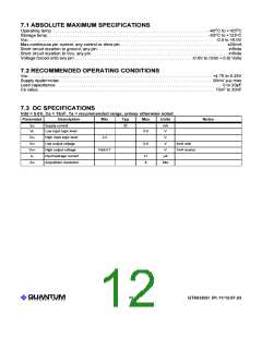
7.1 ABSOLUTE MAXIMUM SPECIFICATIONS
Operating temp. . . . . . . . . . . . . . . . . . . . . . . . . . . . . . . . . . . . . . . . . . . . . . . . . . . . . . . . . . . . . . . . . . . . . . . -40OC to +105OC
Storage temp. . . . . . . . . . . . . . . . . . . . . . . . . . . . . . . . . . . . . . . . . . . . . . . . . . . . . . . . . . . . . . . . . . . . . . . . . -55OC to +125OC
V
DD. . . . . . . . . . . . . . . . . . . . . . . . . . . . . . . . . . . . . . . . . . . . . . . . . . . . . . . . . . . . . . . . . . . . . . . . . . . . . . . . . . . . -0.5 to +6.0V
Max continuous pin current, any control or drive pin. . . . . . . . . . . . . . . . . . . . . . . . . . . . . . . . . . . . . . . . . . . . . . . . 20mꢀ
Short circuit duration to ground, any pin. . . . . . . . . . . . . . . . . . . . . . . . . . . . . . . . . . . . . . . . . . . . . . . . . . . . . . . . . . . infinite
Short circuit duration to VDD, any pin. . . . . . . . . . . . . . . . . . . . . . . . . . . . . . . . . . . . . . . . . . . . . . . . . . . . . . . . . . . . . . infinite
Voltage forced onto any pin. . . . . . . . . . . . . . . . . . . . . . . . . . . . . . . . . . . . . . . . . . . . . . . . . . . . . -0.6V to (Vdd + 0.6) Volts
7.2 RECOMMENDED OPERATING CONDITIONS
VDD. . . . . . . . . . . . . . . . . . . . . . . . . . . . . . . . . . . . . . . . . . . . . . . . . . . . . . . . . . . . . . . . . . . . . . . . . . . . . . . . . . . +4.75 to 5.25V
Supply ripple+noise. . . . . . . . . . . . . . . . . . . . . . . . . . . . . . . . . . . . . . . . . . . . . . . . . . . . . . . . . . . . . . . . . . . . . 20mV p-p max
Load capacitance. . . . . . . . . . . . . . . . . . . . . . . . . . . . . . . . . . . . . . . . . . . . . . . . . . . . . . . . . . . . . . . . . . . . . . . . . . . 0 to 20pF
Cs value. . . . . . . . . . . . . . . . . . . . . . . . . . . . . . . . . . . . . . . . . . . . . . . . . . . . . . . . . . . . . . . . . . . . . . . . . . . . . . . . 10nF to 30nF
7.3 DC SPECIFICATIONS
Vdd = 5.0V, Cs = 15nF, Ta = recommended range, unless otherwise noted
Parameter
Description
Min
Typ
Max
Units
Notes
I
DD
Supply current
25
mA
V
V
IL
Low input logic level
High input logic level
Low output voltage
High output voltage
Input leakage current
Acquisition resolution
0.8
V
HL
OL
2.2
V
V
V
0.6
4mA sink
V
OH
Vdd-0.7
V
1mA source
I
IL
1
8
µA
bits
A
R
LQ
12
QT60320D R1.11/12.07.03

 QUANTUM [ QUANTUM RESEARCH GROUP ]