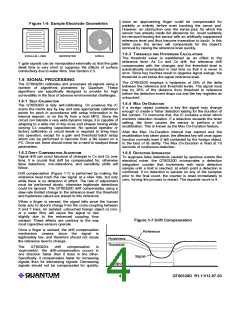
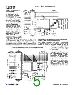
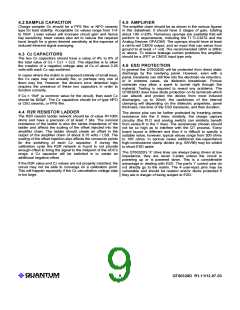
Figure 2-1 Basic QT60320D Circuit
2 - CIRCUIT
Vcc
SPECIFICS
A basic QT60320D circuit is
shown in Figure 2-1.
Keymatrix
5
17 27 29 38
DS1811
Y4
Y3
Y2
Y1
V
V
V
V
V
4
9
40
41
42
43
44
1
Rst
X1
X2
X3
X4
X5
X6
X7
X8
UART IN
Rx
Tx
2.1 SIGNAL PATH
UART OUT 10
The QT60320D requires an
external sampling capacitor,
two Cz capacitors, an amplifier,
some analog switches, and an
R2R ladder DAC to operate.
33
34
35
36
I1
I2
I3
I4
2
3
11
12
13
14
23
24
25
26
R2R dac 100K
O1
O2
O3
O4
O5
O6
O7
O8
19
20
YS1
YS2
The Cs capacitor performs the
charge integration function by
collecting charge coupled
though a selected key during
the dV/dt of the rising edge of
an 'X' scan line. The charge is
sampled 'n' times during the
course of a burst of switching
cycles of length 'n'. As the
burst progresses the charge on
Cs increases in a staircase
fashion (Figure 1-4).
21
22
YS3
YS4
8
C6 (Cz1) 820pF
C7 (Cz2) 820pF
XT1
XT2
74AC04
32
CC1
CC2
R3 68K
7
31
8MHz
R5 10K
30
37
Vcc
_
+
CS
CAL LED
15
BSN20
L1
L2
+
_
16
AIN
G
TLC2272
R6 10K
C5 (Cs)
15nF
STAT LED
G
6
G
G
18 28 39
R4 100K
At the burst's end the voltage
on Cs, which is on the order of
a few tenths of a volt, is
between 0 and 5 volts. Between bursts the Cs reset mosfet is
activated to reset the Cs capacitor to ground.
amplified by a gain circuit which includes an offset current
from the R2R ladder DAC driven by the X drive lines. The
offset current from the R2R ladder repositions the output of
the amplifier chain to coincide as closely as possible with the
center span of the 60320's ADC, which can convert voltages
Gain is directly controlled by burst length 'n', amplifier gain
Av, and the values of Cs, Cz1 and Cz2. Only 'n' can be
adjusted on a key by key basis whereas Av and the
capacitances can only be adjusted
for all keys. The amplifier should
typically have a total positive gain
of 100 +/- 20%..
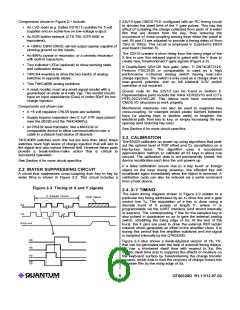
Figure 2-2 Improved Circuit to Suppress Water Films
Vcc
If there is
coupling between X and Y lines,
and where burst length 'n' is set to
a large amount of
Keymatrix
5
17 27 29 38
DS1811
Y4
Y3
Y2
Y1
V
V
V
V
V
4
9
40
41
42
43
44
1
Rst
a
high
number,
charge
X2
X3
X4
X5
X6
X7
X8
UART IN
accumulation on Cs may reach a
point where the ladder DAC can no
longer offset the signal back into
the ADC's usable range. In this
case the circuit will employ one or
two of the Cz capacitors to 'knock
back' or cancel the charge
accumulated on Cs; each Cz will
cancel charge in a discrete step as
required.
Rx
Tx
UART OUT 10
33
34
35
36
I1
I2
I3
I4
2
3
11
12
13
14
23
24
25
26
R2R dac 100K
O1
O2
O3
O4
O5
O6
O7
O8
19
20
YS1
YS2
E
E
E
E
I/O
I/O
I/O
I/O
I/O
I/O
22V10
QS3125
21
22
I/O
I/O
YS3
YS4
Ct
8
C6 (Cz1) 820pF
C7 (Cz2) 820pF
XT1
XT2
Rt
32
CC1
CC2
R3 68K
7
31
8MHz
R5 10K
30
37
Vcc
_
+
CS
CAL LED
15
BSN20
L1
L2
+
_
16
AIN
G
TLC2272
R6 10K
C5 (Cs)
15nF
STAT LED
G
6
G
G
18 28 39
R4 100K
LQ
5
QT60320D R1.11/12.07.03

 QUANTUM [ QUANTUM RESEARCH GROUP ]