push-pull outputs which are sequentially
pulsed in groupings of bursts; a 4-pole
analog switch acts as the sample switch for
all 4 Y lines. At the intersection of each X
and Y line is an interdigitated electrode set
as shown in Figure 1-6. Typically the
outermost electrode is connected to X and
the inner electrode connected to Y.
Remaining Y lines not being sampled are
grounded.
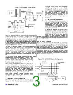
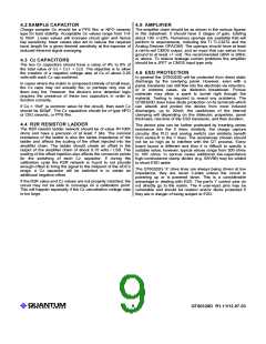
Figure 1-4 QT60320D Circuit Model
Sample
switch (1 of 4)
Y
X drive (1 of 8)
receive line
(1 of 4)
0
Cancellation
switch (1 of 2)
1
Cx
X
electrode
Y
Cz
1
0
electrode
(1 of 2)
Cs
Amp
Reset
switch
1.4 'X' ELECTRODE DRIVES
The 8 'X' lines can be directly connected to
the matrix without buffering. Only the X lines'
positive edges are used to create the
transient field flows used to scan the keys.
Only one X line is active at a time, and it will
pulse for a burst length determined by the
'gain' setting parameter.
X Drive
Reset
switch
8-bit ADC
Sample
switch
If desired an external 22V10 type CMOS
PLD can be used to create the short gate
dwell times necessary to enhance moisture
suppression (Section 1.2). The PLD takes
as its input all 'X' and 'Y' lines, and with
added RC time constants creates the
Amp
V
out
out
0
gain, one of two (or both) Cz capacitors can be switched to
subtract charge from Cs to create a negative-going offset,
bringing the signal back to a usable level. This action occurs
during the course of the burst and is not illustrated in the
timing diagram of Figure 1-4. This mechanism has the benefit
of allowing high levels of Cx while remaining highly sensitive
to small changes in charge coupling due to touch; the circuit
permits the designer to create very large, highly interdigitated
touch keys that are very sensitive.
required short dwell time on the Y switches. The code for the
PLD is available freely on the Quantum web site and can also
be found in Section 5.
1.5 'Y' GATE DRIVES
There are 4 'Y' gate drives (Y1..Y4) which are active-high;
only one Y line is used during a burst for a particular key. The
chosen Y line goes high just before an X line transitions high,
and goes low again just after the X line rises. It is used to
gate on an analog switch, such as a 74HC4066, to capture
charge coupled through a key to the sample capacitor Cs.
The large Cs capacitor creates a virtual ground termination,
making the Y lines appear as a low impedance; this
effectively eliminates cross-coupling among Y lines due to
voltage spikes, while dramatically lowering susceptibility to
EMI. The circuit is also highly tolerant of capacitive loading
on the Y lines, since stray C from Y to ground appears
merely as a parallel capacitance to a much larger value of
Cs.
An inverted version of the Y lines can be used to gate
unselected Y lines to ground, to suppress residual cross-key
coupling that might be caused by cross-pickup from adjacent
X drive traces. See Section 2.2.
The QT60320D circuit design maintains high gain levels
independent of Cx or stray coupling C to ground. It also
readily compensates for field-related issues like
electrode design or the composition of the overlying
panel, as it has individual programmable gain and
threshold settings for each key.
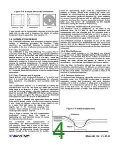
Figure 1-5 QT60320D Matrix Configuration
X drives
Interdigitated
(4 of 8 shown)
keys
Short sample gate dwell times after the X edge can be
used to limit the effect of moisture spreading from key
to key by taking advantage of the RC filter-like nature
of continuous films; the shorter the dwell time, the less
time that the charge has to travel through the
impedance of the film. This effect is completely
independent of the frequency of burst repetition,
intra-burst pulse spacing, or X drive pulse width.
X
X
1
2
X
X
3
4
Y
Y
Y
Y
4
1
2
3
Y
Y
Y
Y
s1
s2
s3
s4
Burst mode operation permits reduced power
consumption and reduces RF emissions, while
permitting excellent response time.
ADC
1.3 MATRIX CONFIGURATION
The matrix scanning configuration is shown in part in
Figure 1-5. The X drives are conventional CMOS
Reset
switch
Cs
LQ
3
QT60320D R1.11/12.07.03

 QUANTUM [ QUANTUM RESEARCH GROUP ]