The SMT components should be oriented perpendicular to
the direction of bending so that they do not fracture when the
PCB is flexed during bonding to the panel.
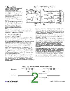
3 Serial Communications
The serial interface is a SPI slave-only mode type which is
compatible with multi-drop operation, i.e. the MISO pin will
float after a shift operation to allow other SPI devices (master
or slave) to talk over the same bus. There should be one
dedicated /SS line for each QT411 from the host controller.
Additional ground area or a ground plane on the PCB will
compromise signal strength and is to be avoided. A single
sided PCB can be made of FR-2 or CEM-1 for low cost.
‘Handshadow’ effects: With thicker and wider panels an
effect known as ‘handshadow’ can become noticeable. If the
capacitive coupling from finger to electrode element is weak,
for example due to a narrow electrode width or a thick, low
dielectric constant panel, the remaining portion of the human
hand can contribute a significant portion of the total
A DRDY (‘data ready’) line is used to indicate to the host
controller when it is possible to talk to the QT411.
3.1 Power-up Timing Delay
Immediately after power-up, DRDY floats for approximately
20ms, then goes low. The device requires ~525ms thereafter
before DRDY goes high again, indicating that the device has
calibrated and is able to communicate.
detectable capacitive load. This will induce an offset error,
which will depend on the proximity and orientation of the hand
to the remainder of the element. Thinner panels and those
with a smaller diameter will reduce this effect since the finger
contact surface will strongly dominate the total signal, and the
remaining handshadow capacitance will not contribute
significantly to create an error offset.
From power up to first communication, allow a total of 550ms
in startup delay.
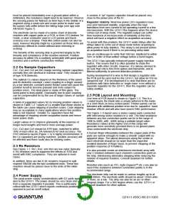
3.2 SPI Timing
PCB Cleanliness: All capacitive sensors should be treated
as highly sensitive circuits which can be influenced by stray
conductive leakage paths. QT devices have a basic
resolution in the femtofarad range; in this region, there is no
such thing as ‘no clean flux’. Flux absorbs moisture and
becomes conductive between solder joints, causing signal
drift and resultant false detections or temporary loss of
sensitivity. Conformal coatings will trap in existing amounts of
moisture which will then become highly temperature
sensitive.
The SPI interface is a five-wire slave-only type; timings are
found in Figure 3-1. The phase clocking is as follows:
Clock idle: High
Data out changes on: Falling edge of CLK from host
Input data read on: Rising edge of CLK from host
Slave Select /SS: Negative level frame from host
Data Ready DRDY: Low from QT inhibits host
Bit length & order: 8 bits, MSB shifts first
Clock rate: 5kHz min, 40kHz max
The designer should specify ultrasonic cleaning as part of the
manufacturing process, and in extreme cases, the use of
conformal coatings after cleaning.
The host can shift data to and from the QT on the same cycle
(with overlapping commands). Due to the nature of SPI, the
return data from a command or request is always one SPI
cycle behind.
An acquisition burst always happens about 920µs after /SS
goes high after coming out of Sleep mode. SPI clocking
lasting more than 15ms can cause the chip to self-reset.
2.6 ESD EMC and Related Issues
,
Please refer to Quantum app note AN-KD02 for further
information on ESD and EMC matters.
Figure 3-1 SPI Timing Diagram
~31ms
~31ms
Acquire Burst
<1ms
<1ms
Sleep Mode
awake
low-power sleep
awake
400us typ
sleep
3-state if left to float
DRDY from QT
>13us, <100us
>12us, <100us
>12us, <100us
>20us
<35us
>1us, <5us
/SS from host
CLK from Host
sleep until automatic wake (~3s)
wake up on /SS line
Data sampled on rising edge
Data shifts out on falling edge
data hold >=12us
after last clock
Host Data Output
?
7
6
5
4
3
2
1
0
0
(Slave Input - MOSI)
command byte
response byte
<10us delay
edge to data
QT Data Output
(Slave Out - MISO)
3-state
3-state
?
7
6
5
4
3
2
1
output driven
<12us after /SS
goes low
output floats
before DRDY
goes low
lQ
6
QT411-ISSG R6.01/1005

 QUANTUM [ QUANTUM RESEARCH GROUP ]