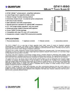
Figure 1-1 QT411 Wiring Diagram
1 Operation
The QT411 uses a SPI slave mode
interface for control and data
communications with a host
Regulator
VIN VOUT
GND
VIN
1
VDD
'RIGHT'
Rs5 8.2k
Rs3 4.7k
C1
2.2uF
C2
5
R1
SNS3B
127
controller. Acquisition timings and
operating parameters are under host
control; there are no option jumpers
and the device cannot operate in a
stand-alone mode.
22k
2.2uF
Cs3
100nF
~400k
6
8
SNS3A
SNS2A
R2
83
45
100k
Cs2
13
DRDY
SDO
/SS
SCLK
SDI
~400k
100nF
2
3
4
The output data is a 7-bit binary
number (0...127) indicating angular
position.
7
SNS2B
SNS1A
R3
1k
SPI BUS
Rs2 4.7k
10
Cs1
~400k
11
100nF
Like all QProx™ devices, the QT411
operates using bursts of
1= Detect Output
12
9
0
DETECT SNS1B
C3
Rs4 8.2k
Rs1 4.7k
'LEFT'
VSS
14
1nF
charge-transfer pulses; burst mode
permits an unusually high level of
control over spectral modulation,
power consumption, and response
time.
If power is not an issue the device can run constantly under
host control, by always raising /SS after 35µs from the last
rising edge of CLK. Constant burst operation can be used by
the host to gather more data to filter the position data further
to suppress noise effects, if required.
The QT411 modulates its bursts in a spread-spectrum
fashion in order to heavily suppress the effects of external
noise, and to suppress RF emissions.
1.1 Synchronized Mode
Synchronized mode also allows the host device to control the
rate of drift compensation, by periodically sending a ‘drift’
command to the device.
Refer also to Figure 3-1, page 6.
Sync mode allows the host device to control the repetition
rate of the acquisition bursts, which in turn govern response
time and power consumption.
In sync mode, the device will wait for the SPI slave select line
/SS to fall and rise and will then do an acquisition burst;
actual SPI clocks and data are optional. The /SS pin thus
becomes a ‘sync’ input in addition to acting as the SPI
framing control.
Mains Sync: Sync mode can and should be used to sync to
mains frequency via the host controller, if mains interference
is possible (ie, running as a lamp dimmer control). The host
should issue SPI commands synchronously with the mains
frequency. This form of operation will heavily suppress
interference from low frequency sources (e.g. 50/60Hz),
which are not easily suppressed using spread-spectrum pulse
modulation.
Within 35µs of the last rising edge of CLK, the device will
enter a low power sleep mode. The rising edge of /SS must
occur after this time; when /SS rises, the device wakes from
sleep, and shortly thereafter does an acquisition burst. If a
more substantial sleep time is desired, /SS should be made
to rise some delay period later.
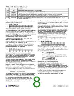
By increasing the amount of time spent in sleep mode, the
host can decrease the average current drain at the expense
of response time. Since a burst typically requires 31ms (at
3.3V, reference circuit), and an acceptable response time
might be ~100ms, the power duty cycle will be 31/100 or 31%
of peak current.
Cross-talk suppression: If two or more QT411’s are used in
close proximity, or there are other QTouch™ type device(s)
close by, the devices can interfere strongly with one another
to create position jitter or false triggering. This can be
suppressed by making sure that the devices do not perform
acquisition bursts at overlapping times. The host controller
can make sure that all such devices operate in distinctly
different timeslots, by using a separate /SS line for each part.
Figure 1-2 Free-Run Timing Diagram ( /SS = high )
~31ms
~31ms
Acquire Burst
<4ms
~30us
DRDY from QT
~25ms
lQ
2
QT411-ISSG R6.01/1005

 QUANTUM [ QUANTUM RESEARCH GROUP ]