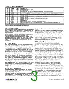
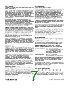
Table 1-1 Pin Descriptions
PIN
NAME
TYPE
DESCRIPTION
1
VDD
Power
Positive power pin (+2.5 .. +5V)
2
SDO
/SS
O
I
I
Serial data output
3
Slave Select pin. This is an active low input that enables serial communications
Serial clock input. Clock idles high
4
SCLK
SNS3B
SNS3A
SNS2B
SNS2A
SNS1B
SNS1A
SDI
5
I/O
I/O
I/O
I/O
I/O
I/O
I
Sense pin (to Cs3, Rs3); connects to both slider ends, each via separate additional 8.2K ohm resistors
Sense pin (to Cs3)
6
7
Sense pin (to Cs2, Rs2); connects to 66% point (from left) of slider
Sense pin (to Cs2)
8
9
Sense pin (to Cs1, Rs1); connects to 33% point (from left) of slider
Sense pin (to Cs1)
10
11
12
13
14
Serial data input
DETECT
DRDY
VSS
O
O
Active high touch detected. May be left unconnected. Note (1)
Data ready output. Goes high to indicate it is possible to communicate with the QT411. Note (1)
Negative power pin
Ground
Note (1): Pin floats ~400µs after wake from Sleep mode.
its state during the 400µs float interval when emerging from
Sleep.
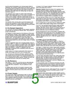
1.2 Free-Run Mode
If /SS stays high, the device will acquire on its own repetitively
after a timeout of about 30ms (Figure 1-2). In this mode, the
DETECT pin can be used to wake up the host when it goes
high upon touch.
Note that in the QT411, detection occurs when one or two of
the sensing channels becomes imbalanced with respect to
the other channel(s). A touch at one position will always
cause such an imbalance. However, a signal change that is
balanced among all 3 channels will not cause a detection. For
example, if a book is placed on top of the slider element, the
channels will all change in the same way and as a result,
detection will be suppressed. This feature is significantly
different from the way the QT401 operates.
In free-run mode, the device does not sleep between bursts.
In this mode the QT411 performs automatic drift
compensation at the maximum rate of one count per 1 20
acquisition burst cycles, or about one count every 7 seconds
without host intervention. It is not possible to change this
setting of drift compensation in Free-Run mode. See also
Section 3.3.3.
1.5 Position Data
The position value is internally calculated and can be
accessed only when the sensor is touched (Detect pin high).
1.3 Sleep Mode
After an SPI transmission, the device will enter a low power
sleep state; see Figure 3-1, page 6, and Section 3.2.4, page
7 for details. This sleep state can be extended in order to
lower average power, by simply delaying the rise of /SS.
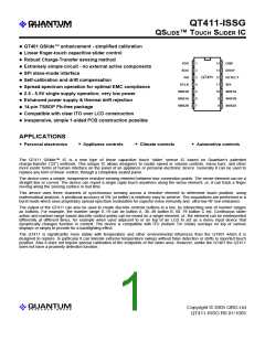
Direction convention: ‘Left’ is defined as the side closest to
the connection made by SNS1, and ‘Right’ is defined as the
side closest to the SNS2 connection. The ends are both
connected to SNS3, each via a resistor which allows the chip
to identify left and right as separate positions. See Figure 1-1.
The use of the terms ‘left’ and ‘right’ should not be interpreted
to mean the device can only be used in one orientation. In
fact the strip can be oriented backwards, vertically, or at any
angle.
Coming out of sleep state when /SS is pulsed, the DETECT
and DRDY pins will float for ~400µs. It is recommended that
the DRDY pin be pulled to Vss with a resistor and DETECT
by bypassed with a capacitor to avoid false signalling if they
are being monitored during this time; see Section 1.4.
Note: Pin /SS clamps to Vss for 250ns after coming out of
sleep state as a diagnostic pulse. To prevent a possible pin
drive conflict, /SS should either be driven by the host as an
open-drain pull-high drive (e.g. with a 100K pullup resistor), or
there should be a ~1K resistor placed in series with the /SS
pin. See Figure 1-1.
The position on the left end reports as 0, while the position at
the right reports as 127. The device reports 45 when touched
at the SNS1 node and 83 at SNS2. The position data is a
7-bit number (0..127) that is computed in real time and is
returned via a status command.
Note that activity on SCLK will also wake the QT411, which
in turn will then wait for the /SS to rise. For lowest possible
operation in Sleep mode, do not pulse on SCLK until after
/SS goes low.
End stops: The QT411 defines end zones of the slider
element as saturated ‘end stops’, which consist of fixed
regions where only a reading of ‘0’ or ‘127’ is returned. This is
to allow robust position detection of these important locations,
so that it is easy for a user to select ‘full off’ and ‘full on’. The
left slider end allocates 10% of the slider’s length to location
‘0’, and the right end similarly allocates 10% of the slider’s
length to location ‘127’. Only the center 80% of the slider’s
length will track changes in touch position in the range of
1..126.
1.4 DETECT Output Pin
This pin drives high when touch is detected and the chip is
reporting an angular position. This condition is also found as
bit 7 in the standard response.
This output will float for ~400µs during wake from Sleep mode
(see Section 1.3). It is recommended that the DETECT pin (if
it is used) be shunted to ground with a 1nF capacitor to hold
The position data will update either with a single rapid touch
or will track if the finger is moved along the surface of the
lQ
3
QT411-ISSG R6.01/1005

 QUANTUM [ QUANTUM RESEARCH GROUP ]