November 2006
rev 1.5
ASM5P2308A
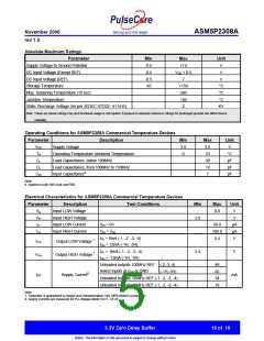
Absolute Maximum Ratings
Parameter
Min
-0.5
-0.5
-0.5
-65
Max
+7.0
VDD + 0.5
7
Unit
V
Supply Voltage to Ground Potential
DC Input Voltage (Except REF)
DC Input Voltage (REF)
V
V
Storage Temperature
+150
260
°C
°C
°C
KV
Max. Soldering Temperature (10 sec)
Junction Temperature
150
Static Discharge Voltage (As per JEDEC STD22- A114-B)
2
Note: These are stress ratings only and functional usage is not implied. Exposure to absolute maximum ratings for prolonged periods can affect device
reliability.
Operating Conditions for ASM5P2308A Commercial Temperature Devices
Parameter
Description
Min
3.0
0
Max
3.6
70
Unit
V
VDD
Supply Voltage
TA
Operating Temperature (Ambient Temperature)
Load Capacitance, below 100MHz
Load Capacitance, from 100MHz to 133MHz
Input Capacitance6
°C
CL
30
pF
pF
pF
CL
10
CIN
7
Note:
6. Applies to both Ref Clock and FBK.
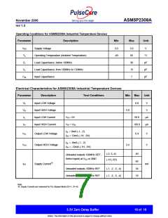
Electrical Characteristics for ASM5P2308A Commercial Temperature Devices
Parameter
Description
Input LOW Voltage
Input HIGH Voltage
Input LOW Current
Input HIGH Current
Test Conditions
Min
Max
0.8
Unit
V
VIL
VIH
IIL
2.0
V
VIN = 0V
50.0
100.0
0.4
µA
µA
V
IIH
VIN = VDD
IOL = 8mA (-1, -2, -3, -4)
IOH = 12mA (-1H, -5H)
VOL
VOH
Output LOW Voltage 7
IOL = -8mA (-1, -2, -3, -4)
IOH = -12mA (-1H, -5H)
2.4
V
Output HIGH Voltage 7
Unloaded outputs 100MHz REF (-2,-3,-4)
49
60
34
18
Select inputs at VDD or GND
(-1H,-5H)
IDD
Supply Current8
mA
Unloaded outputs, 66MHz REF (-1, -2, -3, -4)
Unloaded outputs, 33MHz REF (-1, -2, -3, -4)
Note:
7. Parameter is guaranteed by design and characterization. Not 100% tested in production.
8. Supply Currents are measured for PLL-Bypass Mode (S2=1, S1=0)
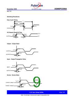
3.3V Zero Delay Buffer
16 of 16
Notice: The information in this document is subject to change without notice.

 PULSECORE [ PulseCore Semiconductor ]