July 2005
rev 1.0
ASM3P623S00A/B/C/D/E/F
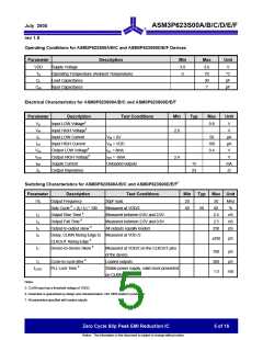
Operating Conditions for ASM3P623S00A/B/C and ASM3P623S00D/E/F Devices
Parameter
Description
Min
3.0
0
Max
3.6
70
Unit
V
VDD
TA
Supply Voltage
Operating Temperature (Ambient Temperature)
Load Capacitance
°C
CL
30
pF
pF
CIN
Input Capacitance
7
Electrical Characteristics for ASM3P623S00A/B/C and ASM3P623S00D/E/F
Parameter
Description
Input LOW Voltage5
Input HIGH Voltage5
Input LOW Current
Input HIGH Current
Output LOW Voltage6
Output HIGH Voltage6
Supply Current
Test Conditions
Min
Typ
Max
0.8
Unit
V
VIL
VIH
IIL
2.0
2.4
V
VIN = 0V
50
100
0.4
µA
µA
V
IIH
VIN = VDD
VOL
VOH
IDD
Zo
IOL = 8mA
IOH = -8mA
V
Unloaded outputs
15
23
mA
Ω
Output Impedance
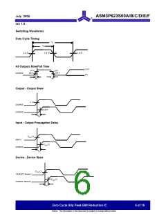
Switching Characteristics for ASM3P623S00A/B/C and ASM3P623S00D/E/F7
Parameter
Description
Test Conditions
Min
Typ
Max Unit
1/t1
Output Frequency
30pF load
20
40
50
60
MHz
%
Duty Cycle 6 = (t2 / t1) * 100
Output Rise Time 6
Measured at VDD/2
50
t3
t4
t5
t6
Measured between 0.8V and 2.0V
Measured between 2.0V and 0.8V
All outputs equally loaded
2.5
2.5
250
nS
nS
pS
Output Fall Time 6
Output-to-output skew 6
Delay, CLKIN Rising Edge to Measured at VDD /2
CLKOUT Rising Edge 6
Device-to-Device Skew 6
±350
pS
t7
Measured at VDD/2 on the CLKOUT pins
of the device
700
200
1.0
pS
pS
tJ
Cycle-to-cycle jitter 6
PLL Lock Time 6
Loaded outputs
tLOCK
Stable power supply, valid clock presented
on CLKIN pin
mS
Notes:
5. CLKIN input has a threshold voltage of VDD/2
6. Parameter is guaranteed by design and characterization. Not 100% tested in production
7. All parameters specified with loaded outputs.
Zero Cycle Slip Peak EMI Reduction IC
5 of 16
Notice: The information in this document is subject to change without notice.

 PULSECORE [ PulseCore Semiconductor ]