July 2005
ASM3P623S00A/B/C/D/E/F
rev 1.0
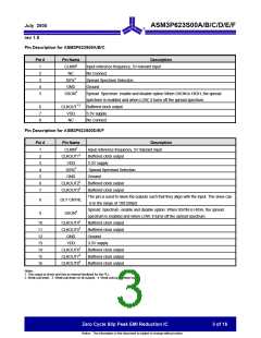
Pin Description for ASM3P623S00A/B/C
Pin #
Pin Name
CLKIN2
NC
Description
1
2
3
4
5
Input reference frequency, 5V-tolerant input
No Connect
SS%4
Spread Spectrum Selection
GND
SSON4
Ground
Spread Spectrum enable and disable option When SSON is HIGH, the spread
spectrum is enabled and when LOW, it turns off the spread spectrum.
6
7
8
CLKOUT1,3
VDD
Buffered clock output
3.3V supply
NC
No Connect
Pin Description for ASM3P623S00D/E/F
Pin #
Pin Name
CLKIN2
Description
Input reference frequency, 5V tolerant input
1
2
3
4
5
6
7
CLKOUT13
VDD
Buffered clock output
3.3V supply
SS%4
Spread Spectrum Selection
GND
Ground
CLKOUT23
CLKOUT33
Buffered clock output
Buffered clock output
The pin is used to skew the outputs such that they align with the input. The skew can
is in the range of 100-200pS
8
9
DLY CNTRL
Spread Spectrum enable and disable option. When SSON is HIGH, the spread
spectrum is enabled and when LOW, it turns off the spread spectrum.
SSON4
10
11
12
13
14
15
16
CLKOUT43
CLKOUT53
GND
Buffered clock output
Buffered clock output
Ground
VDD
3.3V supply
CLKOUT63
CLKOUT73
CLKOUT83
Buffered clock output
Buffered clock output
Buffered clock output
Notes:
1. This output is driven and has an internal feedback for the PLL.
2. Weak pull-down. 3. Weak pull-down on all outputs. 4. Weak pull-up on these inputs.
Zero Cycle Slip Peak EMI Reduction IC
3 of 16
Notice: The information in this document is subject to change without notice.

 PULSECORE [ PulseCore Semiconductor ]