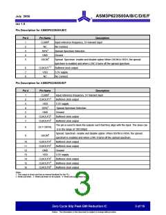
July 2005
rev 1.0
ASM3P623S00A/B/C/D/E/F
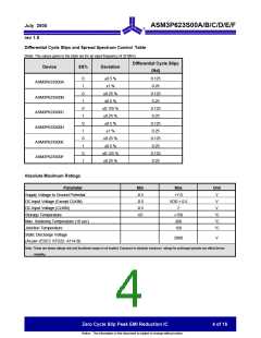
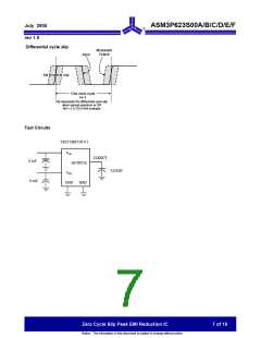
Differential Cycle Slips and Spread Spectrum Control Table
(Note: The values given in the table are for an input frequency of 32 MHz)
Differential Cycle Slips
Device
SS%
Deviation
(Nd)
0.125
0.25
0
1
0
1
0
1
0
1
0
1
0
1
±0.5 %
±1 %
ASM3P623S00A
ASM3P623S00B
ASM3P623S00C
ASM3P623S00D
ASM3P623S00E
ASM3P623S00F
±0.25 %
±0.5 %
±0.125 %
±0.25 %
±0.5 %
±1 %
0.125
0.25
0.125
0.25
0.125
0.25
±0.25 %
±0.5 %
±0.125 %
±0.25 %
0.125
0.25
0.125
0.25
Absolute Maximum Ratings
Parameter
Min
-0.5
-0.5
-0.5
-65
Max
+7.0
Unit
V
Supply Voltage to Ground Potential
DC Input Voltage (Except CLKIN)
DC Input Voltage (CLKIN)
VDD + 0.5
7
V
V
Storage Temperature
+150
260
°C
°C
°C
Max. Soldering Temperature (10 sec)
Junction Temperature
150
Static Discharge Voltage
(As per JEDEC STD22- A114-B)
2000
V
Note: These are stress ratings only and functional usage is not implied. Exposure to absolute maximum ratings for prolonged periods can affect device
reliability.
Zero Cycle Slip Peak EMI Reduction IC
4 of 16
Notice: The information in this document is subject to change without notice.

 PULSECORE [ PulseCore Semiconductor ]